. 2022 Mar 31;17(3):e0264846.
doi: 10.1371/journal.pone.0264846. eCollection 2022.

Sparse CNT networks with implanted AgAu nanoparticles: A novel memristor with short-term memory bordering between diffusive and bipolar switching

Affiliations

Sparse CNT networks with implanted AgAu nanoparticles: A novel memristor with short-term memory bordering between diffusive and bipolar switching

Maik-Ivo Terasa et al. PLoS One. .

Abstract

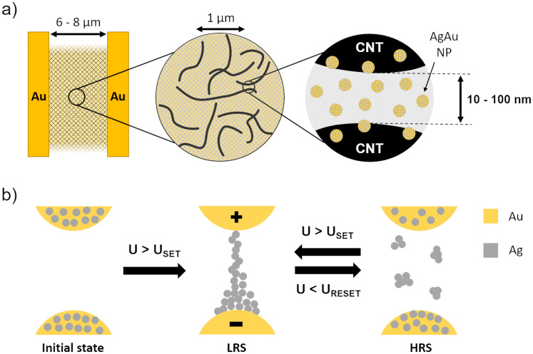
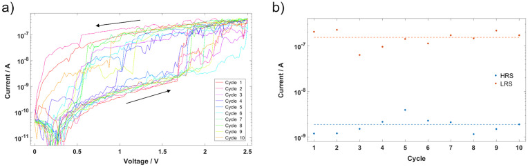
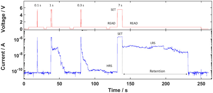
With this work we introduce a novel memristor in a lateral geometry whose resistive switching behaviour unifies the capabilities of bipolar switching with decelerated diffusive switching showing a biologically plausible short-term memory. A new fabrication route is presented for achieving lateral nano-scaled distances by depositing a sparse network of carbon nanotubes (CNTs) via spin-coating of a custom-made CNT dispersion. Electrochemical metallization-type (ECM) resistive switching is obtained by implanting AgAu nanoparticles with a Haberland-type gas aggregation cluster source into the nanogaps between the CNTs and shows a hybrid behaviour of both diffusive and bipolar switching. The resistance state resets to a high resistive state (HRS) either if the voltage is removed with a retention time in the second- to sub-minute scale (diffusive) or by applying a reverse voltage (bipolar). Furthermore, the retention time is positively correlated to the duration of the Set voltage pulse. The potential for low-voltage operation makes this approach a promising candidate for short-term memory applications in neuromorphic circuits. In addition, the lateral fabrication approach opens the pathway towards integrating sensor-functionality and offers a general starting point for the scalable fabrication of nanoscaled devices.


Conflict of interest statement

The authors have declared that no competing interests exist.

Figures

Fig 1
Fig 1. Schematic illustration of the key features and switching mechanism of the CNT/AgAu.
a) Vital components of a CNT/AgAu network from left to right: The inert electrodes, the sparse CNT network and the AgAu nanoparticles inside a nanogap between two individual CNTs. b) The switching mechanism between two NPs when exposed to a potential U. LRS = Low resistive state, HRS = High resistive state.
Fig 2
Fig 2. Percolation measurement for AgAu nanoparticle deposition.
a) Schematic of the in-operando percolation measurement setup. b) Time-resolved current measurement across adjacent electrodes at a voltage of 3V. The time where the flowing current shows a significant increase is taken as the percolation time (337 s). The deposition has been stopped at the percolation point. The red dashed line indicates the progression of the current, if the deposition had continued, leading to an overpercolated layer of nanoparticles.
Fig 3
Fig 3. SEM micrographs of a finished [CNT/AgAu network] without SiN layer.
a+b) Homogeneous sparse CNT network between the electrodes. c) A nanogap between two CNTs with deposited AgAu NP. The samples shown in the images have not been coated with SiN.
Fig 4
Fig 4. Resistive switching behaviour.
a) Cyclic voltage pattern, showing resistive switching behaviour and an ON/OFF ratio of around 81 at a Read voltage of 1.5 V. b) HRS and LRS currents at Read voltage of 1.5 V for each cycle.
Fig 5
Fig 5. Reset behaviour with reverse voltage.
a) Cycle starting in HRS. The LRS is retained until -1.5 V is applied. b) Subsequent cycle starting in LRS. The reset behaviour is symmetrical in the positive and negative voltage range. The numbers indicate in which order the resistive switching occurred.
Fig 6
Fig 6. Time-resolved current measurements showcasing the retention.
The upper graph shows the applied voltage pattern: Read voltage = 0.5 V, Set voltage = 5.5 V. The retention time is taken as the time from returning from Set to Read voltage to when the current reaches the HRS current. The numeric values indicate the duration of the Set voltage pulse. The Set time and retention time show a positive correlation, which can be found in the (see S4 Fig).

References

    1. Chua L. Memristor-The missing circuit element. IEEE Trans. Circuit Theory. 1971; 18: 507–519. doi: 10.1109/TCT.1971.1083337 - DOI
    1. Strukov DB, Snider GS, Stewart DR, Williams RS. The missing memristor found. Nature. 2008; 453: 80–83. doi: 10.1038/nature06932 - DOI - PubMed
    1. Yu S. Neuro-Inspired Computing With Emerging Nonvolatile Memorys. Proc. IEEE. 2018; 106: 260–285. doi: 10.1109/JPROC.2018.2790840 - DOI
    1. Merolla PA, Arthur JV, Alvarez-Icaza R, Cassidy AS, Sawada J, Akopyan F, et al.. Artificial brains. A million spiking-neuron integrated circuit with a scalable communication network and interface. Science. 2014; 345: 668–673. doi: 10.1126/science.1254642 - DOI - PubMed
    1. Vahl A, Carstensen J, Kaps S, Lupan O, Strunskus T, Adelung R, et al.. Concept and modelling of memsensors as two terminal devices with enhanced capabilities in neuromorphic engineering. Sci Rep. 2019; 9: 4361. doi: 10.1038/s41598-019-39008-5 - DOI - PMC - PubMed

Publication types

Substances