. 2022 Apr;8(13):eabm9845.
doi: 10.1126/sciadv.abm9845. Epub 2022 Apr 1.

Nanoscale flexible organic thin-film transistors

Affiliations

Nanoscale flexible organic thin-film transistors

Ute Zschieschang et al. Sci Adv. 2022 Apr.

Abstract

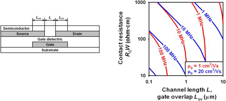
Direct-write electron-beam lithography has been used to fabricate low-voltage p-channel and n-channel organic thin-film transistors with channel lengths as small as 200 nm and gate-to-contact overlaps as small as 100 nm on glass and on flexible transparent polymeric substrates. The p-channel transistors have on/off current ratios as large as 4 × 10⁹ and subthreshold swings as small as 70 mV/decade, and the n-channel transistors have on/off ratios up to 108 and subthreshold swings as low as 80 mV/decade. These are the largest on/off current ratios reported to date for nanoscale organic transistors. Inverters based on two p-channel transistors with a channel length of 200 nm and gate-to-contact overlaps of 100 nm display characteristic switching-delay time constants between 80 and 40 ns at supply voltages between 1 and 2 V, corresponding to a supply voltage-normalized frequency of about 6 MHz/V. This is the highest voltage-normalized dynamic performance reported to date for organic transistors fabricated by maskless lithography.


Figures

Fig. 1.
Fig. 1.. Transit-frequency dependence on TFT parameters.
Contour plot showing the transit frequency (fT) of a field-effect transistor calculated using Eq. 1 for channel lengths (L) and gate-to-contact overlaps (Lov) ranging from 0.1 to 10 μm, channel width–normalized contact resistances (RCW) ranging from 10 ohm·cm to 1 kilohm·cm, and intrinsic channel mobilities (μ0) of 1 and 20 cm2/Vs. The channel length, the gate-to-source overlap, and the gate-to-drain overlap are assumed to be identical (L = Lov = Lov,GS = Lov,GD). The difference between the gate-source voltage (VGS) and the threshold voltage (Vth) was set to a value of 2 V, and the unit-area gate-dielectric capacitance (Cdiel) was set to a value of 0.7 μF/cm2, as these are approximately the values for VGS-Vth and Cdiel that are relevant for the experiments presented in this work. The graph illustrates that, for contact resistances greater than about 100 ohm·cm, the dependence of the transit frequency on the intrinsic channel mobility is relatively weak, while the impact of the critical device dimensions is quite large.
Fig. 2.
Fig. 2.. Device structure.
Schematic TFT cross section and structures of the molecules for organic semiconductors and contact functionalization.
Fig. 3.
Fig. 3.. Flexible nanoscale organic transistors.
(Top row) Photographs of a flexible PEN substrate with an array of 25 organic TFTs fabricated by electron-beam lithography. (Bottom row) Scanning electron microscopy (SEM) images of a TFT having a channel width of 50 μm (left) and of a part of the channel region of a DPh-DNTT TFT having a channel length of 300 nm and gate-to-contact overlaps of 100 nm (right). In the SEM image on the right, the characteristic thin-film morphology of the vacuum-deposited DPh-DNTT films is clearly seen (8, 39).
Fig. 4.
Fig. 4.. Current-voltage characteristics of p-channel DPh-DNTT TFTs fabricated on a flexible PEN substrate.
(Top row) Transfer and output characteristics of a TFT with a channel length of 200 nm, gate-to-contact overlaps of 200 nm, and a channel width of 80 μm. (Bottom row) Transfer characteristics of TFTs with channel lengths of 300, 500, 700, and 900 nm, gate-to-contact overlaps of 100 nm, and a channel width of 50 μm and output characteristics of the TFT with a channel length of 300 nm. The on/off current ratios, subthreshold swings, turn-on voltages, channel width–normalized transconductances, and effective charge-carrier mobilities extracted from the transfer characteristics of these TFTs are summarized in Table 1.
Fig. 5.
Fig. 5.. Low-voltage TFT operation.
Current-voltage characteristics of a p-channel DPh-DNTT TFT with a channel length of 600 nm, gate-to-contact overlaps of 400 nm, and a channel width of 80 μm fabricated on a flexible PEN substrate when operated with maximum gate-source and drain-source voltages of −1 V. The transfer characteristics indicate an on/off current ratio of 3 × 10⁸ and a subthreshold swing of 70 mV/decade.
Fig. 6.
Fig. 6.. Inverters and dynamic performance.
Static and dynamic characteristics of a biased-load unipolar inverter based on two p-channel DPh-DNTT TFTs with channel lengths of 200 nm and gate-to-contact overlaps of 100 nm fabricated on a glass substrate. (Top row) Circuit schematic and static transfer characteristics of the inverter. The drive TFT (connected to VDD) has a channel width of 100 μm (part of the channel region of the drive TFT is shown in the top SEM image), and the load TFT (connected to ground) has a channel width of 20 μm (part of the channel region of the load TFT is shown in the bottom SEM image). The static transfer characteristics indicate a small-signal gain of 2.7. Also shown are the transfer characteristics of an individual TFT with a channel length of 200 nm, gate-to-contact overlaps of 100 nm, and a channel width of 50 μm. (Bottom row) To evaluate the dynamic performance of the TFTs, a square-wave voltage (with an amplitude of 1.0, 1.5, or 2.0 V) is applied to the input node of the inverter, and the output response is measured using an oscilloscope. From the output response, characteristic switching-delay time constants of 80, 60, and 40 ns at supply voltages of 1.0, 1.5, and 2.0 V (equal to the input-voltage amplitude) are extracted for the low-to-high transition of the inverter’s output voltage.
Fig. 7.
Fig. 7.. Transfer and output characteristics of n-channel ActivInk N1100 TFTs fabricated on a glass substrate.
The TFTs have channel lengths of 200, 400, 600, and 800 nm and gate-to-contact overlaps of 150 nm. The channel width is 50 μm. The on/off current ratios, subthreshold swings, turn-on voltages, channel width–normalized transconductances and effective charge-carrier mobilities extracted from the transfer characteristics of these TFTs are summarized in Table 3.

References

    1. Noda M., Kobayashi N., Katsuhara M., Yumoto A., Ushikura S., Yasuda R., Hirai N., Yukawa G., Yagi I., Nomoto K., Urabe T., An OTFT-driven rollable OLED display. J. Soc. Inf. Disp. 19, 316–322 (2011).
    1. Myny K., Beenhakkers M. J., van Aerle N. A. J. M., Gelinck G. H., Genoe J., Dehaene W., Heremans P., Unipolar organic transistor circuits made robust by dual-gate technology. IEEE J. Solid-State Circuits 46, 1223–1230 (2011).
    1. Raiteri D., van Lieshout P., van Roermund A., Cantatore E., Positive-feedback level shifter logic for large-area electronics. IEEE J. Solid-State Circuits 49, 524–535 (2014).
    1. Abdinia S., Ke T.-H., Ameys M., Li J., Steudel S., Vandersteen J. L., Cobb B., Torricelli F., van Roermund A., Cantatore E., Organic CMOS line drivers on foil. J. Disp. Technol. 11, 564–569 (2015).
    1. Ishida K., Huang T.-C., Honda K., Shinozuka Y., Fuketa H., Yokota T., Zschieschang U., Klauk H., Tortissier G., Sekitani T., Toshiyoshi H., Takamiya M., Someya T., Sakurai T., Insole pedometer with piezoelectric energy harvester and 2 V organic circuits. IEEE J. Solid-State Circuits 48, 255–264 (2013).