. 2022 Apr 5;13(1):1851.
doi: 10.1038/s41467-022-29448-5.

Integrated silicon carbide electro-optic modulator

Affiliations

Integrated silicon carbide electro-optic modulator

Keith Powell et al. Nat Commun. .

Abstract

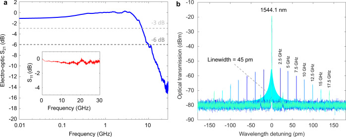
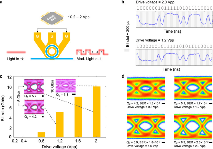
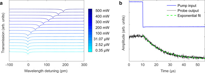
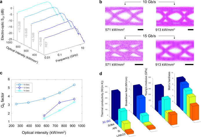
Owing to its attractive optical and electronic properties, silicon carbide is an emerging platform for integrated photonics. However an integral component of the platform is missing-an electro-optic modulator, a device which encodes electrical signals onto light. As a non-centrosymmetric crystal, silicon carbide exhibits the Pockels effect, yet a modulator has not been realized since the discovery of this effect more than three decades ago. Here we design, fabricate, and demonstrate a Pockels modulator in silicon carbide. Specifically, we realize a waveguide-integrated, small form-factor, gigahertz-bandwidth modulator that operates using complementary metal-oxide-semiconductor (CMOS)-level voltages on a thin film of silicon carbide on insulator. Our device is fabricated using a CMOS foundry compatible fabrication process and features no signal degradation, no presence of photorefractive effects, and stable operation at high optical intensities (913 kW/mm2), allowing for high optical signal-to-noise ratios for modern communications. Our work unites Pockels electro-optics with a CMOS foundry compatible platform in silicon carbide.


Conflict of interest statement

The authors declare no competing interests.

Figures

Fig. 1
Fig. 1. Integrated Pockels modulator in SiC on insulator.
a Overview of the fabricated ring modulator showing compatibility with CMOS voltages. b False color SEM of the microring waveguide and modulator electrodes. c False color SEM cross-section of the active region of the modulator. d Simulated static electric field and optical mode of the active region of the modulator. e SEM of an etched waveguide with the sidewall shown. f Measured optical spectrum of the SiC microring resonator after calibrating the optical loss from the VGCs. g Lorentz fit of the resonance line shape to determine the intrinsic optical quality factor (QI) (Cross: Measurement; Solid line: Lorentz fitting).
Fig. 2
Fig. 2. Modulator bandwidth and EO characterization.
a RF s-parameter characterization featuring a −3 dB and −6 dB bandwidths of 7.1 GHz and 9.9 GHz respectively. S21 transmission coefficient of the scattering matrix. Inset shows the S11, reflection spectrum of the modulator. b Optical spectrum at the output of the modulator for various input RF frequencies. The measurement at 2.5 GHz which is within the resonator linewidth is used in the Pockels coefficient extraction.
Fig. 3
Fig. 3. Digital CMOS-level electro-optic modulation with non-return to zero (NRZ) pseudorandom bit sequence (PRBS) of 27 bits.
a Setup configuration using a CMOS DAC to drive the ground-signal-ground (GSG) electrodes of the modulator. b Time-domain waveforms measured at the output of the modulator at 5 Gb/s for drive voltages of 2 Vpp and 1.2 Vpp, respectively. c Drive-voltage-dependent eye diagram quality factors (QE) for increasing bit rate. The bar plot shows the modulation bandwidth with QE > 2.7. The high-bandwidth photodiode is directly connected to a real-time oscilloscope for recording eye diagrams and QE without equalization. No low-pass RF filter is used in the measurement. d Measured eye diagrams and QE at 5 Gbit/s for different drive voltages. A low-pass RF filter is used at the output of the photodiode for inter-symbol-interference reduction. A low-pass RF filter is used at the output of the photodiode for inter-symbol-interference reduction. Eye diagrams and QE are measured via the oscilloscope without equalization. BER is estimated from the measured QE factor,. Scale bars, 33 ps.
Fig. 4
Fig. 4. Transmission spectra and relaxation of SiC resonator at high power.
a Transmission spectra of the probed resonance at 1547 nm with a 1544 nm wavelength pump of varying powers (see colorbar) launching into the VGC to excite the resonator. b Step response showing the probe resonance after the pump beam (500 mW power) is switched off. The exponential decay is due to thermal relaxation.
Fig. 5
Fig. 5. High-power operation and material comparison.
a Electro-optic s-parameter characterization at high optical intensities shows an improvement in RF responses. b Measured eye diagrams at 10 Gb/s and 15 Gb/s. The high-bandwidth photodiode is directly connected to a real-time oscilloscope for recording eye diagrams without equalization. No low-pass RF filter is used in the measurement. Measured eye diagrams confirm increased eye opening and no signal degradation when operating the modulator at high optical intensities. c QE factors as a function of optical intensity for bit rates of 10 Gb/s, 12 Gb/s, and 15 Gb/s show an improved and robust modulation performance for higher input intensity. The high-bandwidth photodiode is directly connected to a real-time oscilloscope for recording eye QE factors without equalization. No low-pass RF filter is used in the measurement. d Material parameter comparison of 3C-SiC with widely used optical materials showing the distinct advantages of SiC for high power handling. Scale bars, 33 picoseconds.

References

    1. Nakamura D, et al. Ultrahigh-quality silicon carbide single crystals. Nature. 2004;430:1009–1012. - PubMed
    1. Lukin DM, et al. 4H-silicon-carbide-on-insulator for integrated quantum and nonlinear photonics. Nat. Photonics. 2020;14:330–334.
    1. Atatüre M, Englund D, Vamivakas N, Lee SY, Wrachtrup J. Material platforms for spin-based photonic quantum technologies. Nat. Rev. Mater. 2018;3:38–51.
    1. Lee TH, Bhunia S, Mehregany M. Electromechanical computing at 500 °C with silicon carbide. Science. 2010;329:1316–1318. - PubMed
    1. Anderson CP, et al. Electrical and optical control of single spins integrated in scalable semiconductor devices. Science. 2019;366:1225–1230. - PubMed