. 2022 May 24;16(5):7210-7232.
doi: 10.1021/acsnano.1c10702. Epub 2022 Apr 6.

Structural Diversity in Multicomponent Nanocrystal Superlattices Comprising Lead Halide Perovskite Nanocubes

Affiliations

Structural Diversity in Multicomponent Nanocrystal Superlattices Comprising Lead Halide Perovskite Nanocubes

Ihor Cherniukh et al. ACS Nano. .

Abstract

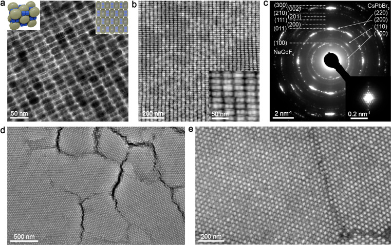
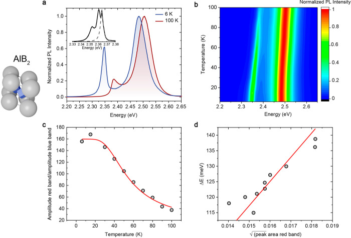
Nanocrystal (NC) self-assembly is a versatile platform for materials engineering at the mesoscale. The NC shape anisotropy leads to structures not observed with spherical NCs. This work presents a broad structural diversity in multicomponent, long-range ordered superlattices (SLs) comprising highly luminescent cubic CsPbBr3 NCs (and FAPbBr3 NCs) coassembled with the spherical, truncated cuboid, and disk-shaped NC building blocks. CsPbBr3 nanocubes combined with Fe3O4 or NaGdF4 spheres and truncated cuboid PbS NCs form binary SLs of six structure types with high packing density; namely, AB2, quasi-ternary ABO3, and ABO6 types as well as previously known NaCl, AlB2, and CuAu types. In these structures, nanocubes preserve orientational coherence. Combining nanocubes with large and thick NaGdF4 nanodisks results in the orthorhombic SL resembling CaC2 structure with pairs of CsPbBr3 NCs on one lattice site. Also, we implement two substrate-free methods of SL formation. Oil-in-oil templated assembly results in the formation of binary supraparticles. Self-assembly at the liquid-air interface from the drying solution cast over the glyceryl triacetate as subphase yields extended thin films of SLs. Collective electronic states arise at low temperatures from the dense, periodic packing of NCs, observed as sharp red-shifted bands at 6 K in the photoluminescence and absorption spectra and persisting up to 200 K.

Keywords: binary superlattice; collective properties; colloidal nanocrystals; electron microscopy; lead halide perovskites; nanocrystal shape; self-assembly.


Conflict of interest statement

The authors declare no competing financial interest.

Figures

Figure 1
Figure 1
Diversity of binary and ternary SLs obtained from 5.3 and 8.6 nm CsPbBr3 nanocubes combined with 11.2–25.1 nm spherical Fe3O4 and NaGdF4 NCs, 10.7–11.7 nm truncated cuboid PbS NCs, thick NaGdF4 disks (31.5 nm in diameter and 18.5 nm thick), and 6.5–28.4 nm disk-shaped LaF3 NCs. Structures in solid and dashed frames were obtained with 8.6 and 5.3 nm CsPbBr3 NCs, respectively. HAADF-STEM image illustrates a sharp shape of a CsPbBr3 nanocube. The graph is a space-filling analysis within a hard-particle model for NaCl-, AlB2-, and AB2- and within OTM for ABO3- and ABO6-type SLs comprising larger spherical and smaller cubic NCs; the dashed line corresponds to the density of fcc packing of spherical NCs.
Figure 2
Figure 2
Binary NaCl-type SL. (a) TEM image, (upper right inset) HAADF-STEM image, along with the corresponding (bottom inset) small-angle and (b) wide-angle ED patterns of a SL domain in [001]SL orientation assembled from 8.6 nm CsPbBr3 cubes and 18.6 nm NaGdF4 NCs. The upper left inset in (a) represents the NaCl-type unit cell according to the preferential cube’s orientation.
Figure 3
Figure 3
Binary and ternary ABO3-type SLs. (a) TEM image along with (b) HAADF-STEM image, (c) the corresponding wide-angle ED pattern, and (d) SEM images of the [001]SL-oriented b-ABO3-type domains assembled from 8.6 nm CsPbBr3 cubes and 16.5 nm NaGdF4 spheres. (e, h) AFM height images of spheres- and cubes-terminated b-ABO3-type domains, respectively, along with (f, i) the height analysis of the profiles indicated in (e, h), (g, j) AFM three-dimensional images with the respective models. (k) TEM image along with (l) HAADF-STEM image, (m) the corresponding wide-angle ED pattern, and (n) SEM image of the [001]SL-oriented b-ABO3-type domains assembled from 8.6 nm CsPbBr3 cubes and 19.8 nm Fe3O4 spheres. (o) TEM image along with (p) HAADF-STEM image and (q) the corresponding wide-angle ED pattern of the [001]-oriented t-ABO3-type SL domains assembled from 8.6 nm CsPbBr3 cubes, 11.7 nm PbS truncated cuboids, and 21.5 nm Fe3O4 spheres. (r) HAADF-STEM image of a t-ABO3-type SL domain in [111]SL orientation assembled from 8.6 nm CsPbBr3, 11.7 nm PbS, and 25.1 nm Fe3O4 NCs; upper inset shows the model of [111]SL-oriented t-ABO3 unit cell, and lower inset shows small-angle ED pattern. Insets in (a, k, o) represent binary and ternary ABO3-type lattices according to the preferential NCs orientations, with Fe3O4 shown as gray spheres, NaGdF4 as yellowish spheres, CsPbBr3 as blue cubes, and PbS as red truncated cubes. The origin of wide-angle ED reflections in (c, m, q) is color-coded to match the NCs in insets.
Figure 4
Figure 4
Binary AlB2-type SLs obtained combining 8.6 nm CsPbBr3 with (a–e) 19.8 nm Fe3O4 and (f–j) 16.5 nm NaGdF4 NCs. (a, b) TEM and (c) HAADF-STEM images of a single domain in [120]SL orientation, along with the corresponding (d) small-angle and (e) wide-angle ED patterns. (f, g) TEM and (h) HAADF-STEM images of a single domain in [001]SL orientation, along with the corresponding (i) small-angle and (j) wide-angle ED patterns. Insets in (e, j) show the orientations of CsPbBr3 NCs in the SL domains with respect to the electron beam (normal to the image plane).
Figure 5
Figure 5
Structural characterization of a binary AlB2-type SL comprising 5.3 nm CsPbBr3 and 12.5 nm Fe3O4 NCs. (a) TEM image of [120]SL-oriented domain; inset is the image at higher magnification. (b) Wide-angle ED pattern of a single SL domain in (a). (c) Two-dimensional GISAX scattering pattern, showing long-range order in AlB2-type binary domains. (d) The unit cell of AlB2-type SL. (e) Small-angle ED pattern of a domain shown in (a). (f) HAADF-STEM image of the [120]SL-oriented domain. (g) EDX-STEM maps for Fe (gray, K-line) and Pb (blue, L-line) of the [120]SL-oriented domain. (h, k, n) Crystallographic models of [120]SL, [001]SL, and [010]SL-oriented AlB2 lattice, respectively. (i, j) Low- and high-magnification TEM images of an [001]SL-oriented domain. (l, m) Low- and high-magnification TEM images of a [010]SL-oriented domain; insets in (i, l) are images obtained by template-matching analysis of corresponding TEM images.
Figure 6
Figure 6
Possible relative orientations of CsPbBr3 nanocubes within AlB2-type SL and packing fractions predicted by OPM packing analysis according to the hard-particle model. In both orientations, the body-diagonal of the cubes is parallel to the c-axis of the hexagonal SL unit cell, that is, [001]SL. In orientation “O1”, the cubes are mutually rotated by 60°, whereas in orientation “O2”, they are identically aligned. A significant increase in the packing fraction can be achieved if the B-cubes in orientation “O2” are not locked in the 2d Wyckoff positions, that is, are allowed to slide along the [001]SL (“O2 S3”). Wide-angle ED patterns from [120]SL- (see, for instance, Figures 4e and 5b) and [001]SL-oriented domains (Figure 5j) point to the alignment of all cubes with one body diagonal parallel to [001]SL and (110) CsPbBr3 planes are orthogonal to [010]SL. Hence these two orientations can be proposed. Experimentally, however, there exists no evidence to differentiate between these two structures, and hence both were considered for the analysis of lattice parameters and packing densities. Excluded is also a substantial orientational disorder in any dimension.
Figure 7
Figure 7
An AB2-type binary SL assembled from CsPbBr3 nanocubes and Fe3O4 nanospheres. (a) TEM image of a SL assembled by 8.6 nm CsPbBr3 and 19.8 nm Fe3O4 NCs (γ = 0.414), along with the corresponding (inset) small-angle ED pattern, (b) HAADF-STEM image, and (c) wide-angle ED pattern. (d) Comparison of AlB2 (taken as orientation “O2”, see Figure 6) and AB2 structures. Red and green lines show the normals to (111) and (110) CsPbBr3 lattice planes, respectively, and indicate the directions of reflections in wide-angle ED patterns. (e) HAADF-STEM image showing grain boundary between AlB2 and AB2 binary SL domains. (f) Modeled crystallographic projections of cubic and spherical NCs in AB2 structure. (g) EDX-STEM elemental maps of an AB2-type binary SL assembled from 5.3 nm CsPbBr3 and 14.5 nm Fe3O4 NCs for Pb (blue, L-line) and Fe (red, K-line).
Figure 8
Figure 8
Binary ABO6-type SLs obtained from 5.3 nm CsPbBr3 and 16.9 nm Fe3O4 NCs (γ = 0.315). (a) Wide-angle and (inset) small-angle ED patterns of [001]SL-oriented domain. (b) Space-filling analysis for b-ABO6-type SLs comprising larger spherical and smaller cubic (solid line) or spherical (blue dashed line) NCs within the hard-particle model, except for the indicated OTM branch. (c) Structural model of a b-ABO6-type unit cell and a slice through (002)SL. (d–f) HAADF-STEM images of [001]SL-, [111]SL-, and [101]SL-oriented domains and (g) the corresponding structural models of SL projections.
Figure 9
Figure 9
Binary SLs self-assembled from the mixtures of 5.3 nm CsPbBr3 and 15.2 nm NaGdF4 NCs. Increasing the relative concentration of CsPbBr3 NCs changes the experiment outcome from (a–d) NaCl-type to (e–h) AlB2-type with (i–l) AB2-type and then to (m, n) ABO3-type SLs, as illustrated by (o) the scheme. (a, e, i, m) TEM images of [001]SL projections, along with the corresponding (bottom insets) small-angle ED and (b, f, j, n) wide-angle ED patterns; the respective high-magnification HAADF-STEM images are shown as upper insets. (c, d) HAADF images of [001]SL- and [111]SL-oriented domains. (g) TEM image of [120]SL-oriented domain, along with the corresponding (upper inset) HAADF-STEM image, (bottom inset) small-angle ED, and (h) wide-angle ED patterns. (k) Bright-field and (l) HAADF-STEM images of [001]SL-oriented domain.
Figure 10
Figure 10
Characterization of b-ABO3-type SL assembled from 8.6 nm CsPbBr3 and 10.7–11.7 nm PbS. (a) HAADF-STEM image of a single [001]SL-oriented binary ABO3 domain comprising of 8.6 nm CsPbBr3 NCs and 11.7 nm PbS NCs. (b) TEM image of a single b-ABO3 domain in [001]SL orientation assembled from 8.6 nm CsPbBr3 NCs and 10.7 nm PbS NCs, together with the respective (c) small-angle and (d) wide-angle ED patterns. Diffraction arcs are colored to show their origin from CsPbBr3 and PbS NCs presented as insets. Inset in (a) shows the binary ABO3 lattice and illustrates the relative position and orientation of NCs. (e) Crystallographic model of a [001]SL-oriented ABO3 lattice, along with HAADF-STEM image and respective EDX-STEM maps for S (red, K-line), Pb (blue, L-line), Cs (green, L-line), and Br (yellow, K-line).
Figure 11
Figure 11
NaCl-type binary SLs from 8.6 nm CsPbBr3 NCs combined with truncated cuboid PbS NCs. (a) TEM image of a monolayer domain. (b, c) HAADF-STEM images of SL domains with an increasing number of layers. (e, f) TEM images of [001]SL-oriented SL domains at different magnification, along with the (g) wide-angle and (h) small-angle ED patterns measured from the domain shown in (f); the reflections from CsPbBr3 and PbS NCs are colored to match the NCs in the structural model (d). Images from (a, c, f–h) were obtained with 10.7 nm PbS NCs (γ = 0.778) and from (b, e) with 11.7 nm PbS NCs (γ = 0.720).
Figure 12
Figure 12
CuAu- and AlB2-type binary SLs assembled from truncated cuboid 10.7 nm PbS NCs and, respectively, 8.6 and 5.3 nm CsPbBr3 cubes. (a) TEM image of a single CuAu-type SL domain in [101]SL orientation, along with the corresponding (inset) small-angle ED and (b) wide-angle ED patterns (the origin of the reflections is color-coded to match the NCs in the model shown as inset). (c) CuAu unit cell and crystallographic model of [101]SL-oriented lattice assuming preferable orientations of NCs in agreement with ED. (d) HAADF-STEM images of a SL domain taken at 0° and 45° tilting angles around [010]SL that correspond to [101]SL and [001]SL orientations, respectively; crystallographic model of [001]SL-oriented CuAu-type lattice is depicted in the inset of (e). (f) EDX-STEM elemental maps recorded from a [001]SL-oriented domain shown in (e). (g) TEM image of AlB2-type SL with twist grain boundaries between [001]SL- (magnified in upper inset) and [010]SL-oriented (magnified in bottom inset) domains. (h) HAADF-STEM, high-magnification TEM image (upper inset), and crystallographic model (bottom inset) along with (i) wide-angle ED pattern of [120]SL-oriented AlB2-type SL. Bottom and upper ([120]SL orientation) insets in (i) represent the unit cell of AlB2-type SL with orientations of NCs that result in the most intense wide-angle ED spots marked in red (PbS) and blue (CsPbBr3).
Figure 13
Figure 13
CaC2-like SL assembled from 8.6 nm CsPbBr3 nanocubes and 31.5 nm NaGdF4 thick nanodisks, featuring sets of two cubes on one lattice site. (a) TEM image and the SL models are shown as insets. (b) HAADF-STEM images at different magnifications, along with the corresponding (c) wide-angle ED and (inset) small-angle ED patterns. (d, e) SEM images at different magnifications.
Figure 14
Figure 14
Binary SLs obtained from FAPbBr3 nanocubes. (a) TEM and HAADF-STEM (top right panel) images of a b-ABO3-type SL assembled from 9 nm FAPbBr3 and 19.5 nm NaGdF4 NCs; SL model is shown in the bottom right panel. (b, c) Bright-field STEM images of, respectively, an [120]-oriented AlB2-type and [001]SL-oriented AB2-type SL domains comprising 9 nm FAPbBr3 and 15.1 nm NaGdF4 NCs. (d) HAADF-STEM image of an [111]-oriented NaCl-type SL domain comprising 5.7 nm FAPbBr3 and 15.1 nm NaGdF4 NCs. (e) Bright-field STEM image of a columnar AB-type SL domain obtained from 5.7 nm FAPbBr3 NCs and 12.5 nm LaF3 nanodisks. (f) TEM and (g) HAADF-STEM images of lamellar SL obtained from 5.7 nm FAPbBr3 NCs and 12.5 nm LaF3 nanodisks; EDX-STEM elemental maps for La (magenta, L-line) and Pb (blue, L-line) are shown in the inset in (g). Insets in (b–d) are SL models.
Figure 15
Figure 15
Self-assembly of perovskite NCs at the liquid–air interface. (a) Illustration of the assembly process: NCs dispersed in nonpolar solvents are cast onto the surface of glyceryl triacetate in a Teflon well or Petri dish, which is then covered with glass or larger Petri dish, respectively; ordered SL film floating on the subphase is formed upon evaporation the solvent. (b–d) TEM images of 9 nm CsPbBr3 NC monolayer obtained from octane on glyceryl triacetate. (e–g) TEM images of AB-type monolayer (obtained from dodecane) and NaCl- and AlB2-type films (obtained from decane), respectively, comprising 8.6 nm CsPbBr3 and 19.8 nm Fe3O4 NCs.
Figure 16
Figure 16
Oil-in-oil templated assembly of binary SLs comprising perovskite NCs. (a) Illustration of the assembly process: NCs dispersed in toluene are mixed with a fluorinated solvent (FC-40) containing surfactant (008-FS) that is capable of stabilizing droplets with NCs. Slow evaporation of toluene from the droplets during stirring results in the formation of ordered binary supraparticles. (b) SEM and HAADF-STEM (right panel) images of supraparticles with b-ABO3 structure obtained from 8.6 nm CsPbBr3 cubic and 18.6 nm NaGdF4 spherical NCs. (c) SEM images of supraparticles with CaC2-like structure assembled from 8.6 nm CsPbBr3 nanocubes and 31.5 nm NaGdF4 thick nanodisks. Insets in (b, c) show the SL models.
Figure 17
Figure 17
PL properties of ABO3-type binary SLs at 6 K. (a) PL spectra of binary ABO3-type SLs assembled by employing 8.6 nm CsPbBr3 and 19.5 nm (top) or 14.5 nm (bottom) Fe3O4 NCs. The PL spectra (black solid lines) are fitted to a doubled Lorentzian function (red and blue lines are the individual functions, while the gray lines are the cumulative fits to the experimental data). (b) Measured coupled vs uncoupled splitting energy for several samples with different distances between O-site and B-site NCs. Error bars denote the standard deviation obtained by measuring several PL spectra on different locations on the same sample.
Figure 18
Figure 18
Impact of the temperature on the PL band from coupled NCs in AlB2-type binary SLs (5.3 nm CsPbBr3 NCs + 12.5 nm Fe3O4 NCs). (a) Normalized PL spectra for the AlB2-type SLs at 6 and 100 K. The inset reports a zoom-in PL spectrum for a nominally similar sample where much narrower emission peaks are resolved (full width at half-maximum of about 3 meV, dashed line). (b) Two-dimensional colored plot of normalized PL spectra obtained at different temperatures. (c) The relative amplitude of the two emission bands as a function of temperature (black open circles). The red solid line is the best fit to an Arrhenius plot returning activation energy of 14 meV, very close to the LO-phonon energy of CsPbBr3 crystal (17 meV). (d) Extracted splitting energy is plotted vs the squared root of the red-shifted peak area, exhibiting a linear dependence (solid red line).
Figure 19
Figure 19
PL and absorbance spectra of binary ABO3-type SLs comprising 8.8 nm CsPbBr3 cubes and 18.2 nm (top panel) or 15.1 nm (middle panel) NaGdF4 spherical NCs, measured at 10 K (top and middle panel) and 200 K (bottom panel).

Similar articles

Cited by

References

    1. Boles M. A.; Engel M.; Talapin D. V. Self-Assembly of Colloidal Nanocrystals: From Intricate Structures to Functional Materials. Chem. Rev. 2016, 116, 11220–11289. 10.1021/acs.chemrev.6b00196. - DOI - PubMed
    1. Tan R.; Zhu H.; Cao C.; Chen O. Multi-Component Superstructures Self-Assembled from Nanocrystal Building Blocks. Nanoscale 2016, 8, 9944–9961. 10.1039/C6NR01662F. - DOI - PubMed
    1. Urban J. J.; Talapin D. V.; Shevchenko E. V.; Kagan C. R.; Murray C. B. Synergism in Binary Nanocrystal Superlattices Leads to Enhanced P-Type Conductivity in Self-Assembled PbTe/Ag2Te Thin Films. Nat. Mater. 2007, 6, 115–121. 10.1038/nmat1826. - DOI - PubMed
    1. Chen J.; Ye X.; Oh S. J.; Kikkawa J. M.; Kagan C. R.; Murray C. B. Bistable Magnetoresistance Switching in Exchange-Coupled CoFe2O4-Fe3O4 Binary Nanocrystal Superlattices by Self-Assembly and Thermal Annealing. ACS Nano 2013, 7, 1478–1486. 10.1021/nn3052617. - DOI - PubMed
    1. Ye X.; Chen J.; Diroll B. T.; Murray C. B. Tunable Plasmonic Coupling in Self-Assembled Binary Nanocrystal Superlattices Studied by Correlated Optical Microspectrophotometry and Electron Microscopy. Nano Lett. 2013, 13, 1291–1297. 10.1021/nl400052w. - DOI - PubMed