Review
. 2022 Mar 22;12(7):1043.
doi: 10.3390/nano12071043.

Functional Devices from Bottom-Up Silicon Nanowires: A Review

Affiliations
Review

Functional Devices from Bottom-Up Silicon Nanowires: A Review

Tabassom Arjmand et al. Nanomaterials (Basel). .

Abstract

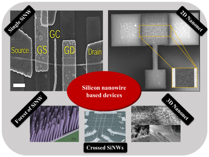
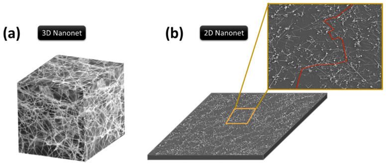
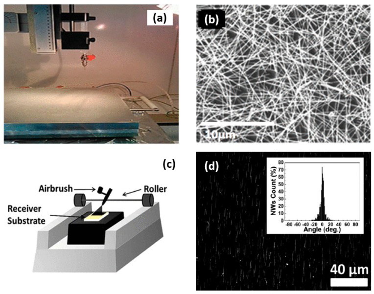
This paper summarizes some of the essential aspects for the fabrication of functional devices from bottom-up silicon nanowires. In a first part, the different ways of exploiting nanowires in functional devices, from single nanowires to large assemblies of nanowires such as nanonets (two-dimensional arrays of randomly oriented nanowires), are briefly reviewed. Subsequently, the main properties of nanowires are discussed followed by those of nanonets that benefit from the large numbers of nanowires involved. After describing the main techniques used for the growth of nanowires, in the context of functional device fabrication, the different techniques used for nanowire manipulation are largely presented as they constitute one of the first fundamental steps that allows the nanowire positioning necessary to start the integration process. The advantages and disadvantages of each of these manipulation techniques are discussed. Then, the main families of nanowire-based transistors are presented; their most common integration routes and the electrical performance of the resulting devices are also presented and compared in order to highlight the relevance of these different geometries. Because they can be bottlenecks, the key technological elements necessary for the integration of silicon nanowires are detailed: the sintering technique, the importance of surface and interface engineering, and the key role of silicidation for good device performance. Finally the main application areas for these silicon nanowire devices are reviewed.

Keywords: integration process; nanonets; nanowires; silicon; transistor.


Conflict of interest statement

The authors declare no conflict of interest. The funders had no role in the design of the study; in the collection, analyses, or interpretation of data; in the writing of the manuscript, or in the decision to publish the results.

Figures

Figure 1
Figure 1
Number of articles published per year and the number of citations based on a search using the keyword “Si or Silicon Nanowire” on the website Of Knowledge.
Figure 2
Figure 2
Different types of nanowire-based samples [33,34].
Figure 3
Figure 3
Schematic made by SEM images for representation of a nanonet (a) three-dimensional (3D nanonet) and (b) two-dimensional (2D nanonet). A top view and percolation path in red are highlighted in image (b).
Figure 4
Figure 4
The major advantage of 1D nanostructures (B) over 2D thin film (A). Binding to 1D nanowire leads to depletion or accumulation in the ‘bulk’ of the nanowire as opposed to only the surface in the 2D thin-film case. Reproduced from [61].
Figure 5
Figure 5
Silicon nanowire nanonets manufactured by vacuum filtration and then transferred to (a) Silicon/Si3N4, (b) Kapton, (c) plastic, and (d) glass substrates. (e) The transmittance of SiNN with the three densities were shown in image (e), the transmittance of the substrate (bare glass) is also reported. Reproduced from [114].
Figure 6
Figure 6
SEM image and fluctuation range in the current of (a) single nanowire and (b) nanonet-based resistors. Reproduced from ref. [28].
Figure 7
Figure 7
Schematic representation of two bottom-up synthesis methods. (A) Vapour-Liquid-Solid Chemical Vapor Deposition (VLS-CVD). Segmentation in composition is possible by the modulation of the gaseous precursor. (B) Electrochemical deposition in solution into anodic aluminum oxide. Segmentation is also possible.
Figure 8
Figure 8
Schematic of the growth principle of SiNWs, and SEM image of as grown silicon nanowires Reproduced from [125].
Figure 9
Figure 9
Assembly of periodic NW arrays and layer-by-layer assembly of crossed NW arrays. (A) Schematic view of the assembly of NWs onto a chemically patterned substrate. The light gray areas correspond to NH2-terminated surfaces, whereas the dark gray areas correspond to either methyl-terminated or bare surfaces. NWs are preferentially attracted to the NH2-terminated regions of the surface. (B) Parallel arrays of GaP NWs with 500-nm separation obtained with a patterned SAM surface. (C) Typical SEM images of crossed arrays of InP NWs obtained in a two-step assembly process with orthogonal flow directions for the sequential steps. Flow directions are highlighted by arrows in the images. (D) An equilateral triangle of GaP NWs obtained in a three-step assembly process, with 60° angles between flow directions, which are indicated by numbered arrows. The scale bars correspond to 500 nm in (BD) Reproduced from [130].
Figure 10
Figure 10
Langmuir−Blodgett assembly of nanowires. (a) Schematic illustration of the Langmuir−Blodgett assembly process. Reproduced from [134]. (b,c) SEM images of a high-density parallel nanowire array (b) and crossed nanowire array (c) on the substrates. (d) SEM images at different magnifications for patterned crossed nanowire arrays. Reproduced from [43].
Figure 11
Figure 11
Illustration of blown bubble films method and photographs of the directed bubble expansion process in the early and final stages. Reproduced from [137].
Figure 12
Figure 12
Illustration of printing apparatus. Reproduced from [139].
Figure 13
Figure 13
Schematics and demonstration of nano-combing. (a) Schematics of the nano-combing process. The blue arrow indicates the traveling direction of the growth substrate with respect to the target substrate, which yields a combing/aligning force that is parallel and opposite to the anchoring force. The dashed window at the right bottom shows a side view of the nano-combing process. (b,c) SEM images of silicon nanowires on the combing (resist) surface at different magnifications. The thickness of the resist (S1805) layer was 70 nm. Scale bars: 50 μm (b), 10 μm (c) Reproduced from [144].
Figure 14
Figure 14
(ad) Friction-based SCCP concept. (a) Schematic illustration of a nanowire in mechanical contact with a surface. The frictional force is predominantly influenced by the shear velocity vector, applied load, contact morphology, and materials of the nanowire and the target substrate. (bd) Optical microscopy images of nanowires transferred in a lubricant-free manner (exemplified by the solid arrow in (a)) onto Si3N4, SiO2, and Au surfaces. The dashed arrow represents the shear direction of the growth substrate. (ei) Influence of local surface features on SCCP. (e) Schematic illustration showing the interaction of a nanowire with a previously deposited nanowire (left), the interactions of nanowires with a step (center), and the interaction of a nanowire with a nanoparticle (right). (f) Schematic and optical images of an 80 nm step in Si3N4, revealing that nanowires are preferentially deposited onto the elevated area. (g) Optical micrograph depicting an area decorated locally with Au nanoparticles of 50 nm in diameter. The nanoparticles increase the frictional force acting on the nanowires and, therefore, significantly increase the deposited nanowire density. (h) SEM image of a nanowire on a surface decorated with Au nanoparticles of 20 nm in diameter. The arrows indicate the positions of nanoparticles. The inset shows a magnified region containing a nanowire and Au nanoparticles. (i) The effect of the step, as shown in (f), is masked when Au nanoparticles (here, 50 nm in diameter) are present. The shear direction of the growth substrate is indicated in all images by a dashed arrow. The scale bars for (fi) represent 100 μm, and that for (h) represents 1 μm. (jm) Towards SCCP nano-device fabrication. (j) Schematic illustration of various catcher concepts, listed from front to back: elevated plateaux, nanoparticles, changes in surface roughness or material composition, catchers with selectivity or guiding rails, catchers for single and multiple-nanowire positioning, and catchers fabricated out of the substrate material with nanowires spanning a trench. (k) Catchers on SiO2 of different lateral shapes, leading to an increased nanowire density adjacent to the catcher. The dashed arrow indicates the shear direction of the nanowire growth substrate. (l) Gold catchers on Si3N4 with the ability to position single nanowires (see white arrows). The width of a single structure is 300 nm. (m) Optical image of one triangular and six rectangular Au structures for single-nanowire positioning. When the triangular structure catches a single nanowire, the rectangular structures appear to assist, serving a function similar to that of a guiding rail, as revealed by experiments. Reproduced from [143].
Figure 15
Figure 15
Overview of the protocol for manufacturing nanonets. This process consists of five main steps: (1) dispersion of the silicon NWs in solution, (2) purification of the NW suspension by centrifugation, (3) analysis of the suspension by absorption spectroscopy, (4) assembly of the NWs into nanonets by vacuum filtration, and (5) transfer of the nanonet onto a substrate. Reproduced from [27].
Figure 16
Figure 16
Membranes obtained after vacuum filtration of nanowires having the same arbitrarily fixed absorbance (0.06 at 400 nm) and different filtered volumes (a) 10 mL, (b) 20 mL, and (c) 35 mL. Reproduced from [28].
Figure 17
Figure 17
(a) Image of the electrostatic spray system step. Reproduced from [159]. (b) SEM image of the electrostatic spray deposited nanowire network. Reproduced from [159]. (c) Schematic of the spray coating apparatus. Reproduced from [158]. (d) representative dark-field optical image of spray-coated SiNWs on the SiOx/Si substrate and the constituent analysis of 700 SiNWs with respect to the flow direction. Reproduced from [158]. Spray coating method can be controlled under conditions of temperature, droplet size, spray coating angle, and airflow which makes this method interesting either in the well-aligned or well controlled density in large size of nanonet with a small lack in control over the low density of nanonets.
Figure 18
Figure 18
Continued scaling of silicon complementary metal–oxide–semiconductor (CMOS) transistor into nanometer regime requires the corresponding reduction in device active layer dimensionality. Reproduced from [6].
Figure 19
Figure 19
(a) Simple comparison between single SiNW-, thin film Si- and SiNN-FETs with respect to the industrial size and fabrication costs related. (b) Positioning (Nanonet TFT) in terms of thin-film transistor (TFT) performance versus footprint in comparison with the existing technologies (TFT based on: cSi: monocrystalline Si; poly-Si: polycrystalline Si; a-Si: amorphous Si; Organic: organic material; Oxide: metal oxide film).
Figure 20
Figure 20
Schematic of NWFETS with (a) back gate, (b) semi-cylindrical top gate, and (c) cylindrical gate-all-around configurations. The nanowire is brown, gate-dielectric is light green, and source (S), drain (D), and top-gate (G) electrodes are gold. Insets show device cross section at the midpoint between source and drain.
Figure 21
Figure 21
(i) The growth of SiNWs in CVD reaction via the VLS mechanism. (ii) Deposition/alignment of SiNWs on a silicon substrate. (iii) A photomask pattern to define source/drain electrodes. (iv) Thermal evaporation to deposit the source/drain contacts. (v) Lift-off the remaining photoresist with Remover PG. Adapted from [174].
Figure 22
Figure 22
(a) Schematic and (b) SEM image of SiNN transistor studied. The schematic (a) refers to long channel transistors for which the length of the NWs (LNFs) is less than the channel length (Lc). Conversely, the SEM image (b) refers to the possible conduction paths involving NW–NW junctions are indicated in red. Reproduced from [27].
Figure 23
Figure 23
Main steps in the isolation of nanonets. (i-0) Fabrication of nanonets. (i-1) Deposition of the positive photoresist by the spin-coating technique. (i-2) Photolithography with the UV–visible through the mask. (i-3) Photoresist development. (i-4) Dry etching of the NWs by a sulfur hexafluoride plasma. (i-5) Photoresist removal. Main steps for the formation of source/drain contacts. (ii-0) Nanonet after isolation. (ii-1) Deposition of inversion photoresist using the spin-coating technique. (ii-2) Photolithography in the UV–visible through the mask aligned with the isolated nanonet. (ii-3) Photoresist development. (ii-4) Electron beam evaporation of nickel and gold. (ii-5) Revelation of the source/drain contacts after lifting of the photoresist (lift-off).
Figure 24
Figure 24
(a) SEM image final full back-gate FET based on SiNN. The length of the Si nanonet channel is 50 μm for a width of 120 μm. The square contacts measure 200 μm on each side. (b) SEM image final local top-gate FET based on SiNN. The length of the Si nanonet channel is 50 μm for a width of 100 μm. The square contacts measure 200 μm on each side. Although this integration process involves only simple and mastered steps, such integration has proven to be challenging since, to date, very few papers have presented the fabrication of this type of device. Moreover, to date, there are works based on the SiNN devices on rigid substrates, especially resistors and transistors but there is a great potential in the field of flexibility that is still unproven.
Figure 25
Figure 25
(a) Schematics of bottom-gate of multi parallel array silicon nanowires. Reproduced from [177] (b) SEM image of as fabricated parallel channels FETs with intruded NiSi2 Schottky barrier contacts. Reproduced from [178]. (c) Refer to the schematic of the short channel transistor (Nanowire length higher than channel length) (d) SEM image of MPC-FETs based on short-channel SiNN and the possible conduction paths involving with without-NW–NW junctions are indicated in red. Reproduced from [27].
Figure 26
Figure 26
SiNW-FETs: a family of current versus drain-source voltage (Ids-Vds) plots for a representative (a) 20 nm p-Si NW device (channel length of 1 µm; from red to pink, Vg = −5 V to 3 V); and (b) 20 nm n-Si NW device (channel length of 2 µm; from yellow to red, Vg = −5 V to 5 V) in a standard back-gated NW-FET geometry as illustrated. Insets in (a,b) are current versus gate–voltage (Ids-Vg) curves recorded for NWFETs plotted on linear (blue) and log (red) scales at Vds = −1 V and 1 V, respectively. Reproduced from [31].
Figure 27
Figure 27
Sensing properties. (A,B) Real-time recordings of the absorption/desorption processes of F1-ATPases, showing the gradual changes in ID with three steps. Drain voltage, VD = 0.1 V and gate voltage, VG = 0 V. (C,D) Corresponding AFM images after protein delivery ((C), inset shows an enlarged image of a single F1 protein) and after further EDTA treatment ((D) inset is the height profile of the bare silicon nanowire and the nanowire with an adsorbed F1 protein particle in (C) inset. The total height of F1 is ~12 nm including a ~2 nm linkage). The scale bar is 1 µm. Reproduced from [75].
Figure 28
Figure 28
(a) Source-drain voltage Vsd versus a gate voltage Vg statistics of 36 nanowire parallel array FET devices. Each device consists of 500–1000 nanowires. Off-current versus on-current per mm electrode width for Vsd = 0.5 V. The on/off ratio is shown for devices with four different inter-electrode spacing but the same silicidation process (green/stars 2.5 µm; red/triangles 3.5 µm; purple/circles 4.5 µm; blue/sq. 5.5 µm). Reproduced from [178]. (b) High density nanowires are contacted by nickel electrodes. The inset displays the histogram of channel lengths of individual nanowires after silicidation for a device with 2.5 µm inter-electrode spacing. Reproduced from [178].
Figure 29
Figure 29
Study of transistor electrical properties for various channel lengths. (A) Typical transfer characteristics from 5 to 100 μm at Vd = −4 V. (B) On current (Ion) as a function of off current (Ioff). The on current is defined as Id at Vg = −25 V, Vd = −4 V, (C) subthreshold slope (SS), and (D) threshold voltage (Vth) for various channel lengths extracted for about seventy transistors. For (B) the on-to-off ratio (Ion/Ioff) is indicated by the dashed lines. Reproduced from [72].
Figure 30
Figure 30
Typical transfer characteristic at Vd = −1 V for single SiNW-FET with Lc = 3 μm (black), MPC-FET with Lc = 5 μm (blue), SiNN-FET with Lc = 50 μm (red). Reproduced from [72].
Figure 31
Figure 31
A comparison between single SiNW-FETs [11,33,175,181,182,183,184,185,186,187,188,189,190] and SiNN-FETs with respect to the channel length (SiNN density is about 0.6 NWs μm−2). Squares of SiNN-FETs segment show the average of several devices’ performances in which bars are representative of deviation in measured parameters for a certain Lc.
Figure 32
Figure 32
(a) Evolution of the conductance over time of Si nanonets based on not-annealed degenerated NWs and annealed at 400 °C after deoxidation. The conductance at 5 V was normalized to the initial conductance just after deoxidation. (b) Diagrams illustrating, after deoxidation, the reoxidation under air of an NW–NW junction (1.a) without annealing or (1.b) with annealing at 400 °C under nitrogen. Reproduced from [27].
Figure 33
Figure 33
(a.1) High-resolution TEM image realized after re-oxidation of a junction between two NWs annealed at 400 °C under nitrogen. (a.2) Schematic representation of the TEM image showing the formation of a dislocation and a neck delimited by SiO2 at the NW–NW junction. (b.1) Modeling of the sintering between two silicon nanoparticles with (w/) and without (w/o) the native oxide. Surface diffusion (js), volume diffusion from the grain boundary (jL), and vapor diffusion (jv) are the material transports considered. X and φ represent the shot size and diameter of the nanoparticles, respectively. (b.2) Sintering map representing the neck size relative to the initial nanoparticle size as a function of temperature for different annealing times. Reproduced from [48].
Figure 34
Figure 34
Comparison between sintered SiNN coated by (A,C) natively grown silicon dioxide and passivated by (B,D) alumina deposited using ALD. (A, B) Refer to top-view SEM images of nanonets, while (C, D) are sectional schemes of three coated SiNWs: one sectioned in the length and two according to the diameter. For (C), the mean and standard deviation of SiNW length (LSiNWs) and diameter (DSiNWs) are indicated. For (D), due to conformal coating with ALD, alumina is deposited simultaneously on SiNWs and onto the substrate whereas SiNW–SiNW junction and underneath SiNW portions are considered alumina-free. Reproduced from [47].
Figure 35
Figure 35
(A) Effect of the alumina thickness on the subthreshold slope (SS). 0 nm of alumina corresponds to a 2-nm thick layer of native SiO2. For all transistors, the channel length (Lc) is 20 μm and the drain voltage (Vd) was set at −4 V. The boxes show the 25th and 75th percentiles, whereas the whiskers represent the 5th and 95th percentiles. The empty square in the boxes shows the mean value. (B) Reproducibility of the on and off current for transistors based on native SiO2 SiNNs (full symbol) and 8-nm alumina encapsulated SiNNs (empty symbol) for 20 μm (square) and 30 μm (triangle) long channel. For native SiO2 SiNN based devices, no current is observed when the channel length is 30 μm. The on-to-off ratio (Ion = Ioff) is indicated by the dashed line. Ion and Ioff were extracted at −25 V and +25 V, respectively. Reproduced from [47].
Figure 36
Figure 36
(a) SEM image of the Si nanonet (NN) after transfer on heavily doped Si substrate covered with a 200 nm thick Si3N4. (b) High-resolution TEM (HRTEM) image displaying an Al2O3 passivated Si nanowire. (c) Optical image of Al2O3 passivated SiNN field effect transistors (FETs) presenting different channel geometries. (d) Transfer characteristics were obtained for an L = 100 μm, W = 100 μm NN-FET at a drain voltage of Vds = −2 V before and after functionalization with thrombin-binding aptamer (TBA-15). Reproduced from [200].
Figure 37
Figure 37
Schematic structure of the devices with MPTS as anchoring layer for gold electrodes. Reproduced from [201].
Figure 38
Figure 38
Vt as a function of the channel modification. Reproduced from [201].
Figure 39
Figure 39
Binary phase diagram of the nickel–silicon pair. Reproduced from [209].
Figure 40
Figure 40
Temperature range of formation of different NiXSiy silicides in SiNWs reported in the literature from 15 references [175,176,182,213,214,216,217,218,219,220,221,222,223,224].
Figure 41
Figure 41
(a) SEM view of a silicided contact after annealing at 400 °C under nitrogen gas during 300 s. The scale bar is 80 nm. (b) EDX picture of the contact presented in (a). Green color indicates the presence of nickel. One can notice the propagation of the nickel in the SiNW after the annealing step leading to the formation of a silicide. (c) Length of the silicided section obtained at 400 °C under nitrogen gas in an RTA furnace as a function of the annealing time. Reproduced from [11].
Figure 42
Figure 42
Transfer characteristics before and after silicidation (400 °C, for 60 s) of a 20 μm channel Si nanonet FET elaborated with 18 mL of filtered SiNW solution (with 42 × 106 NWs cm−2 corresponding density). The drain-source bias was set at −4 V. Reproduced from [226].
Figure 43
Figure 43
(a) Optical images and (b) schematic illustration of the SiNW CMOS inverter on a transparent substrate. Reproduced from [234]. (c) Schematic of a SiNW-FET-based charge-trapping non-volatile flash memory; (d) TEM image of the cross section of a MATATOS device. Inset demonstrates the typical thickness of the top gate stack. Reproduced from [231].
Figure 44
Figure 44
(a.1) The illustration of a nanoscale FET biosensor with a cross-sectional view. (b.1) When positively charged target molecules bind the receptor modified on a p-type NW, positive carriers (holes) are depleted in the NW, resulting in a decrease in conductance. Conversely, negatively charged target molecules captured by the receptor would make an accumulation of hole carriers, causing an increase in conductance. Reproduced from [174]. (a.2) Schematic of a single virus binding and unbinding to the surface of a SiNW device modified with antibody receptors and the corresponding time-dependent change in conductance. (b.2) Simultaneous conductance and optical data recorded for a Si nanowire device after the introduction of influenza A solution. The images correspond to the two binding/unbinding events highlighted by time points 1–3 and 4–6 in the conductance data, with the virus appearing as a red dot in the images. Reproduced from [17].
Figure 45
Figure 45
Real time current response of Pd coated SiNWs in 5% H2. The inset images show the enlarged current response (upper) and an SEM image (below) of the device. Note that, the sensor was inside a chamber with a pressure of 0.01 Torr, and a voltage of 2 V was applied across it. Reproduced from [236].

References

    1. Ramgir N.S., Yang Y., Zacharias M. Nanowire-Based Sensors. Small. 2010;6:1705–1722. doi: 10.1002/smll.201000972. - DOI - PubMed
    1. Wu B., Heidelberg A., Boland J. Mechanical properties of ultrahigh-strength gold nanowires. Nat. Mater. 2005;4:525–529. doi: 10.1038/nmat1403. - DOI - PubMed
    1. Rosaz G. Intégration 3D de Nanofils Si et SiGe Pour la Réalisation de Transistors Verticaux à Canal. 2012. [(accessed on 9 February 2022)]. Available online: https://www.theses.fr/2012GRENT108.
    1. Lu W., Xiang J. Semiconductor Nanowires: From Next-Generation Electronics to Sustainable Energy. [(accessed on 8 February 2022)];R. Soc. Chem. 2015 39 Available online: http://stacks.iop.org/0022-3727/39/i=21/a=R01.
    1. Liu L.-C., Huang M.-J., Yang R., Jeng M.-S., Yang C.-C. Curvature effect on the phonon thermal conductivity of dielectric nanowires. J. Appl. Phys. 2009;105:104313. doi: 10.1063/1.3130671. - DOI

LinkOut - more resources