. 2022 Apr 4;22(7):2770.
doi: 10.3390/s22072770.

Two High-Precision Proximity Capacitance CMOS Image Sensors with Large Format and High Resolution

Affiliations

Two High-Precision Proximity Capacitance CMOS Image Sensors with Large Format and High Resolution

Yuki Sugama et al. Sensors (Basel). .

Abstract

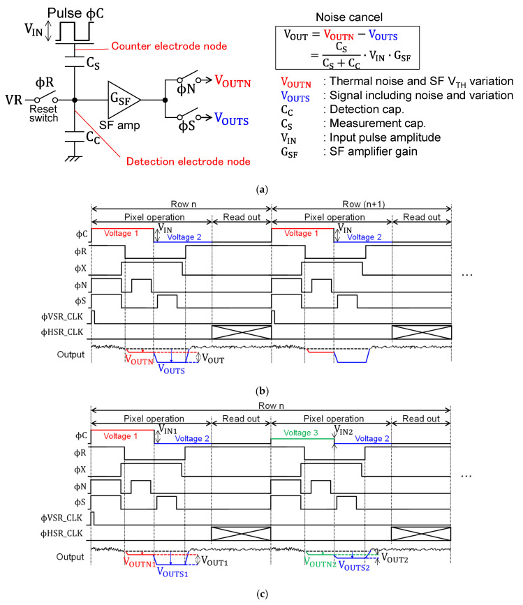
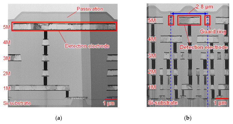
This paper presents newly developed two high-precision CMOS proximity capacitance image sensors: Chip A with 12 μm pitch pixels with a large detection area of 1.68 cm2; Chip B with 2.8 μm pitch 1.8 M pixels for a higher resolution. Both fabricated chips achieved a capacitance detection precision of less than 100 zF (10-19 F) at an input voltage of 20 V and less than 10 zF (10-20 F) at 300 V due to the noise cancelling technique. Furthermore, by using multiple input pulse amplitudes, a capacitance detection dynamic range of up to 123 dB was achieved. The spatial resolution improvement was confirmed by the experimentally obtained modulation transfer function for Chip B with various line and space pattens. The examples of capacitance imaging using the fabricated chips were also demonstrated.

Keywords: CMOS; high precision; high resolution; image sensor; large format; proximity capacitance.


Conflict of interest statement

The authors declare no conflict of interests.

Figures

Figure 1
Figure 1
The 3D models of the sensor and the target, and the captured images for each target: (a) conductive target; (b) dielectric target; (c) particulate targets.
Figure 2
Figure 2
The schematics of the two chips: (a) the circuit block diagram; (b) the circuit schematic of the pixels.
Figure 3
Figure 3
Principle of operation of proximity capacitance image sensor: (a) simplified circuit and noise cancelling principle; (b) timing diagram of normal mode; (c) timing diagram of HDR mode.
Figure 4
Figure 4
The pixel layout diagrams of the two chips: (a) up to the 1st metal layer of Chip A; (b) up to the 1st metal layer of Chip B; (c) the top metal layer.
Figure 5
Figure 5
The micrograph of the fabricated CMOS proximity capacitance image sensors: (a) Chip A; (b) Chip B.
Figure 6
Figure 6
The cross-sectional pixel TEM image of the two chips: (a) Chip A; (b) Chip B.
Figure 7
Figure 7
The measurement system for characterizing the performance of fabricated sensor chips: (a) picture; (b) block diagram.
Figure 8
Figure 8
Various assembly methods of the sensor chips: (a) ceramic package with bonding wires; (b) resin potting; (c) polyimide film with flexible wires.
Figure 9
Figure 9
Captured images without and with noise cancelling and their histograms in the absence of targets: (a) Chip A; (b) Chip B.
Figure 10
Figure 10
Measurement to determine the capacitance value of CC: (a) sensor chip irradiated with light; (b) pulse timing; (c) histogram of measured CC of Chip B and CC values of the two chips.
Figure 11
Figure 11
Measured transfer characteristics of the two chips: (a) measurement methods; (b) Chip A; (c) Chip B.
Figure 12
Figure 12
Calculation of capacitance and distance detection precision: (a) cross-sectional schematic diagram of a chip surface and a conductor target with small irregularities; (b) calculation results of the relation between the measurement capacitance CS and the capacitance detection precision ΔCSmin at each input voltage VIN; (c) relation between the reference distance x between the chip surface and the target and the distance detection precision Δxmin.
Figure 13
Figure 13
Resolution measurement of Chip B: (a) cross-sectional structure of the chip with metal wiring created on the surface; (b) captured images of the wiring for each pitch; (c) output signal for each pixel when 20 µm pitch wiring captured by Chip B; (d) MTF calculated from the measurement results.
Figure 14
Figure 14
Captured image of a fingerprint by the large format Chip A (blurred for privacy).
Figure 15
Figure 15
Captured images of a general-purpose logic IC (TC74HC02): (a) captured by optical image sensor using a microscope; (b) captured by Chip A; (c) captured by Chip B.
Figure 16
Figure 16
Comparison of images captured of a general-purpose IC chip with the sensor operating in normal mode and HDR mode: (a) Normal mode; (b) HDR mode.
Figure 17
Figure 17
Captured images of a drop of saline solution on the sensor surface drying out as time advances captured by Chip B: (a) sample images; (b) closed-up images of red rectangle in (a).
Figure 18
Figure 18
Captured images of printed circuit board wiring by optical image sensor and Chip A: (a) no defects; (b) open defect; (c) short defect. φC was applied only to the center wire indicated by the red arrows.
Figure 19
Figure 19
Captured image of flat panel display with a line defect by Chip A.
Figure 20
Figure 20
Benchmark comparison with other sensors [6,9,10,11,12,13,14,15,16,17,18,19,20,21,22,23,26]: (a) comparison of detection precision and pixel area; (b) comparison of detection precision and pixel pitch and examples of target.

Similar articles

Cited by

References

    1. Sukhavasi S.B., Sukhavasi S.B., Elleithy K., Abuzneid S. Abdelrahman Elleithy CMOS Image Sensors in Surveillance System Applications. Sensors. 2021;21:488. doi: 10.3390/s21020488. - DOI - PMC - PubMed
    1. Ohta J. Smart CMOS Image Sensors and Applications. CRC Press; Boca Raton, FL, USA: 2020.
    1. Oike Y. Imaging Devices and Systems for Future Society; Proceedings of the 2020 IEEE International Electron Devices Meeting (IEDM) Tutorial; Virtual. 12-16 December 2020.
    1. Viable Cell Density Sensors Process Analytics Hamilton Company. [(accessed on 7 February 2022)]. Available online: https://www.hamiltoncompany.com/process-analytics/sensors/cell-density-s....
    1. CCMT-10D CCMT-D Series Ceramic Capacitance Manometer Transducer Type Vacuum Gauge Products ULVAC SHOWCASE. [(accessed on 7 February 2022)]. Available online: https://showcase.ulvac.co.jp/en/products/vacuum-gauge/transducer-type-g-....

LinkOut - more resources