

The Magnetic Genome of Two-Dimensional van der Waals Materials
- PMID: 35442017
- PMCID: PMC9134533
- DOI: 10.1021/acsnano.1c09150
The Magnetic Genome of Two-Dimensional van der Waals Materials
Abstract
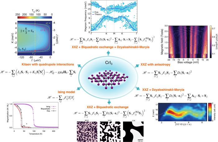
Magnetism in two-dimensional (2D) van der Waals (vdW) materials has recently emerged as one of the most promising areas in condensed matter research, with many exciting emerging properties and significant potential for applications ranging from topological magnonics to low-power spintronics, quantum computing, and optical communications. In the brief time after their discovery, 2D magnets have blossomed into a rich area for investigation, where fundamental concepts in magnetism are challenged by the behavior of spins that can develop at the single layer limit. However, much effort is still needed in multiple fronts before 2D magnets can be routinely used for practical implementations. In this comprehensive review, prominent authors with expertise in complementary fields of 2D magnetism (i.e., synthesis, device engineering, magneto-optics, imaging, transport, mechanics, spin excitations, and theory and simulations) have joined together to provide a genome of current knowledge and a guideline for future developments in 2D magnetic materials research.
Keywords: 2D magnetic materials; CrI3; Fe3GeTe2; atomistic spin dynamics; magnetic genome; magneto-optical effect; neutron scattering; van der Waals.
Conflict of interest statement
The authors declare no competing financial interest.
Figures
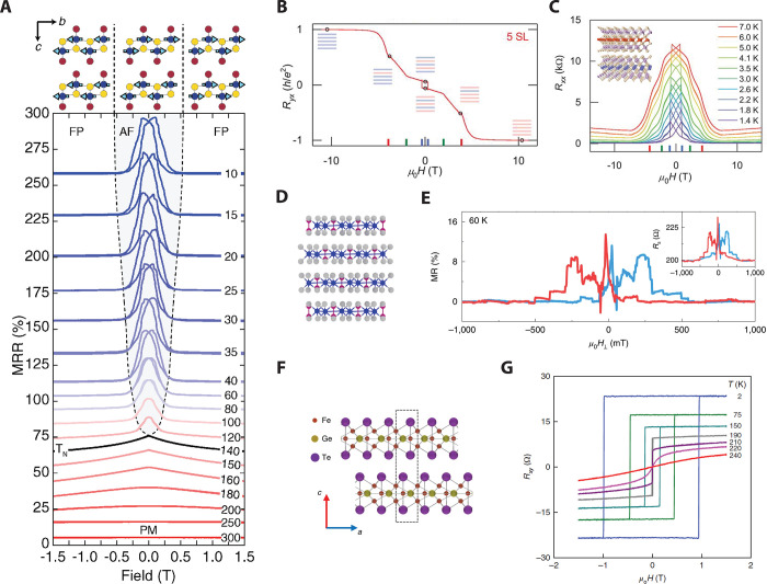
 in bulk CrSBr versus magnetic
field (parallel to the b-axis) at various temperatures.
Each MRR curve is offset for clarity. The solid black line is an MRR
curve taken near the Néel temperature. The antiferromagnetic
(AF), fully polarized (FP), and paramagnetic (PM) phases are labeled,
and the phase boundary is denoted by dashed black lines. Schematics
showing the orientation of the spins in the AF and FP states are given
above the plot. Reproduced with permission
from ref (110). Copyright
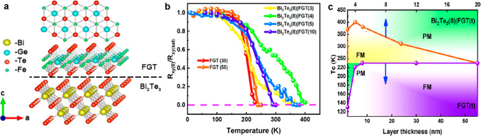
2020 John Wiley and Sons. (B) Ryx of a 5-layer MnBi2Te4 sample as a function
of external magnetic field applied perpendicular to the sample plane
at T = 1.6 K. Data are symmetrized to remove the Rxx component. (C) Rxx of
a 5-layer MnBi2Te4 flake as a function of magnetic
field acquired at various temperatures. Data are symmetrized to remove
the Ryx component. Inset
shows the layered crystal structure of MnBi2Te4 in the AF state. Panels (B) and (C)
are reproduced with permission from ref (111). Copyright 2020 AAAS. (D) Ball and stick model
of the Cr2Ge2Te6 crystal structure. (E) Magnetoresistance
in bulk CrSBr versus magnetic
field (parallel to the b-axis) at various temperatures.
Each MRR curve is offset for clarity. The solid black line is an MRR
curve taken near the Néel temperature. The antiferromagnetic
(AF), fully polarized (FP), and paramagnetic (PM) phases are labeled,
and the phase boundary is denoted by dashed black lines. Schematics
showing the orientation of the spins in the AF and FP states are given
above the plot. Reproduced with permission
from ref (110). Copyright
2020 John Wiley and Sons. (B) Ryx of a 5-layer MnBi2Te4 sample as a function
of external magnetic field applied perpendicular to the sample plane
at T = 1.6 K. Data are symmetrized to remove the Rxx component. (C) Rxx of
a 5-layer MnBi2Te4 flake as a function of magnetic
field acquired at various temperatures. Data are symmetrized to remove
the Ryx component. Inset
shows the layered crystal structure of MnBi2Te4 in the AF state. Panels (B) and (C)
are reproduced with permission from ref (111). Copyright 2020 AAAS. (D) Ball and stick model
of the Cr2Ge2Te6 crystal structure. (E) Magnetoresistance  curves
for T = 60 K and
back-gate voltage of 3.9 V for a 22 nm-thick Cr2Ge2Te6 flake. The background is removed for clarity.
The magnetic field is applied in the out-of-plane direction. Unprocessed
data are shown in the inset. Panels (D)
and (E) are reproduced with permission from ref (86). Copyright 2020 Springer
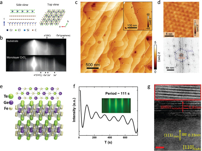
Nature. (F) Side view of the atomic lattice of bilayer Fe3GeTe2. The dashed rectangular box denotes the crystal
unit cell. (G) Temperature-dependent
magnetic field (out-of-plane) sweeps of the Hall resistance measured
on a 12 nm thick Fe3GeTe2 flake. Panels (F) and (G) are reproduced with permission
from ref (77). Copyright
2018 Springer Nature.
curves
for T = 60 K and
back-gate voltage of 3.9 V for a 22 nm-thick Cr2Ge2Te6 flake. The background is removed for clarity.
The magnetic field is applied in the out-of-plane direction. Unprocessed
data are shown in the inset. Panels (D)
and (E) are reproduced with permission from ref (86). Copyright 2020 Springer
Nature. (F) Side view of the atomic lattice of bilayer Fe3GeTe2. The dashed rectangular box denotes the crystal
unit cell. (G) Temperature-dependent
magnetic field (out-of-plane) sweeps of the Hall resistance measured
on a 12 nm thick Fe3GeTe2 flake. Panels (F) and (G) are reproduced with permission
from ref (77). Copyright
2018 Springer Nature.
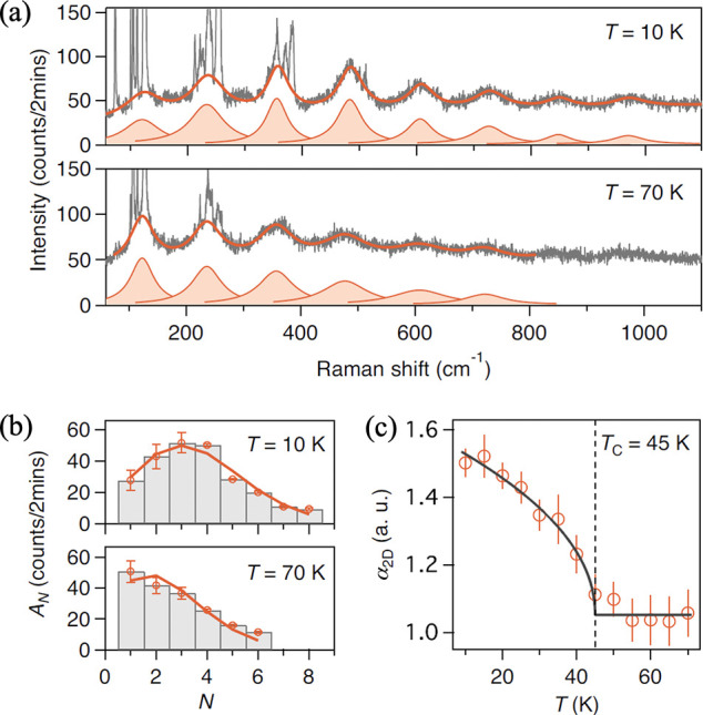
 . (b) Histogram plot of
the fitted Lorentzian
mode intensity (AN) as
a function of N at 10 and 70 K. Solid curves are
fits of the peak intensity profiles to the Poisson distribution functions,
. (b) Histogram plot of
the fitted Lorentzian
mode intensity (AN) as
a function of N at 10 and 70 K. Solid curves are
fits of the peak intensity profiles to the Poisson distribution functions,  . (c)
Plot of 2D e-ph coupling constant
(α2D) as a function of temperature.
The dashed vertical line marks the magnetic onset TC = 45 K. Adapted with permission under
a Creative Commons CC BY license from ref (220). Copyright 2020 Springer Nature.
. (c)
Plot of 2D e-ph coupling constant
(α2D) as a function of temperature.
The dashed vertical line marks the magnetic onset TC = 45 K. Adapted with permission under
a Creative Commons CC BY license from ref (220). Copyright 2020 Springer Nature.
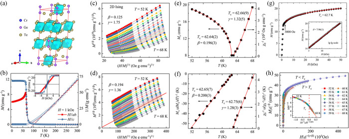
 (right) with solid fitting curves.
(f)
Kouvel–Fisher plots of
(right) with solid fitting curves.
(f)
Kouvel–Fisher plots of  (left) and
  (right) with solid fitting curves. (g)
Isotherm MversusH plot collected at Tc = 62.7 K. Inset: The same plot in log–log scale with a solid
fitting curve. (h) Scaling plots of renormalized magnetization mversus renormalized field h below and above Tc for
Cr2Ge2Te6. Inset: The rescaling of
the M(H) curves by MH–1/δversus εH–1/(βδ).
All panels adapted with permission from ref (279). Copyright 2017 American
Physical Society.
(right) with solid fitting curves. (g)
Isotherm MversusH plot collected at Tc = 62.7 K. Inset: The same plot in log–log scale with a solid
fitting curve. (h) Scaling plots of renormalized magnetization mversus renormalized field h below and above Tc for
Cr2Ge2Te6. Inset: The rescaling of
the M(H) curves by MH–1/δversus εH–1/(βδ).
All panels adapted with permission from ref (279). Copyright 2017 American
Physical Society.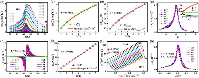
 , (d) δTfwhm,
and (e) RCPversusH with the fitted curves; (f) Modified Arrott plot
based on the obtained critical exponents. Scaling of the |ΔSM(T, H)| curves: (g) normalized ΔSM(T, H)
as a function of θ (inset gives Tr1 and Tr2 as a function of H); (h) – ΔSM/H(1−α)/Δversus ε/H1/Δ. All panels adapted with permission from ref (280). Copyright 1998 American
Physical Society.
, (d) δTfwhm,
and (e) RCPversusH with the fitted curves; (f) Modified Arrott plot
based on the obtained critical exponents. Scaling of the |ΔSM(T, H)| curves: (g) normalized ΔSM(T, H)
as a function of θ (inset gives Tr1 and Tr2 as a function of H); (h) – ΔSM/H(1−α)/Δversus ε/H1/Δ. All panels adapted with permission from ref (280). Copyright 1998 American
Physical Society.
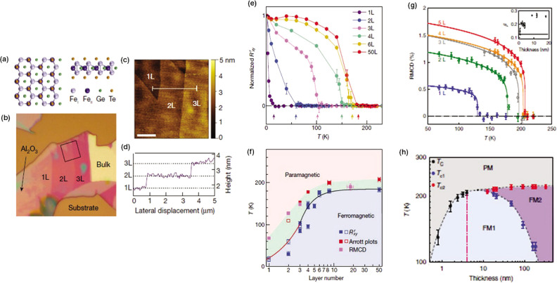
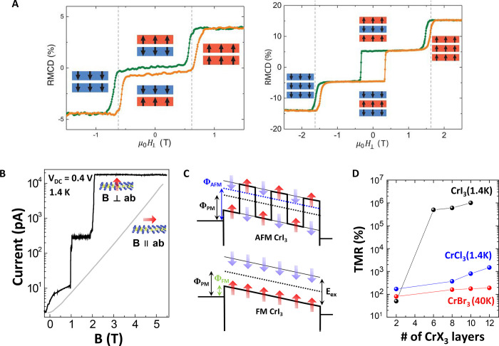
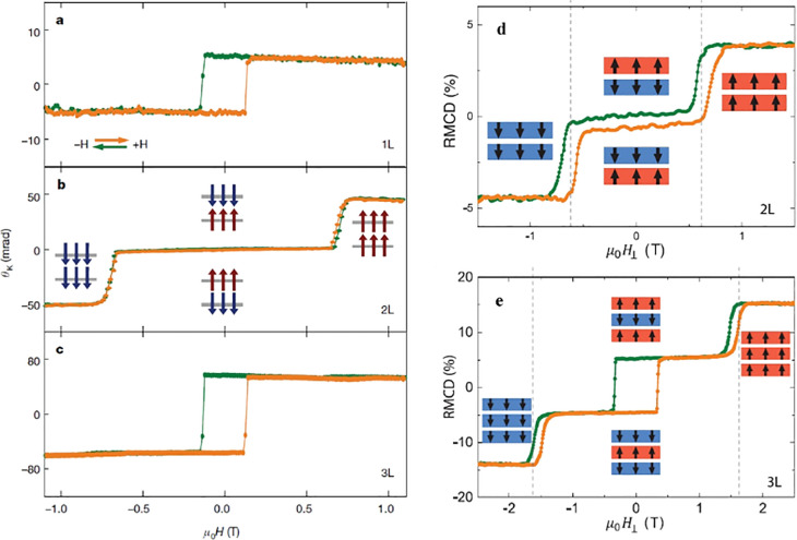
 as a function of temperature obtained from
Fe3GeTe2 thin-flake samples with varying numbers
of layers. Arrows mark the FM transition temperature Tc. (f) Phase diagram of Fe3GeTe2 as layer number and temperature are varied. Tc values are determined from
anomalous Hall effect, Arrott plots and RMCD are displayed in blue,
red and magenta, respectively. (g) Remanent RMCD signal as a function
of temperature for a sequence of selected few-layer flakes (1 L, monolayer;
2 L, bilayer; 3 L, trilayer; 4 L, four layers; 5 L, five layer). The
solid lines are least-squares criticality fits of the form α(1
– T/Tc)β. Inset: derived values of the exponent β plotted as a function
of thickness. (h) Thickness-temperature phase diagram. PM denotes
the region in which the flake is paramagnetic, FM1 that in which it
is FM with a single domain and FM2 that in which the flake exhibits
labyrinthine or stripe domains. The transition temperatures, Tc, Tc1, and Tc2, are based on the temperature-dependent RMCD or anomalous Hall effect
measurements for each flake thickness. The red dashed line denotes
the critical thickness at which a dimensional crossover occurs. All
panels are adapted with permission from ref (12). Copyright 2018 Springer
Nature.
as a function of temperature obtained from
Fe3GeTe2 thin-flake samples with varying numbers
of layers. Arrows mark the FM transition temperature Tc. (f) Phase diagram of Fe3GeTe2 as layer number and temperature are varied. Tc values are determined from
anomalous Hall effect, Arrott plots and RMCD are displayed in blue,
red and magenta, respectively. (g) Remanent RMCD signal as a function
of temperature for a sequence of selected few-layer flakes (1 L, monolayer;
2 L, bilayer; 3 L, trilayer; 4 L, four layers; 5 L, five layer). The
solid lines are least-squares criticality fits of the form α(1
– T/Tc)β. Inset: derived values of the exponent β plotted as a function
of thickness. (h) Thickness-temperature phase diagram. PM denotes
the region in which the flake is paramagnetic, FM1 that in which it
is FM with a single domain and FM2 that in which the flake exhibits
labyrinthine or stripe domains. The transition temperatures, Tc, Tc1, and Tc2, are based on the temperature-dependent RMCD or anomalous Hall effect
measurements for each flake thickness. The red dashed line denotes
the critical thickness at which a dimensional crossover occurs. All
panels are adapted with permission from ref (12). Copyright 2018 Springer
Nature.
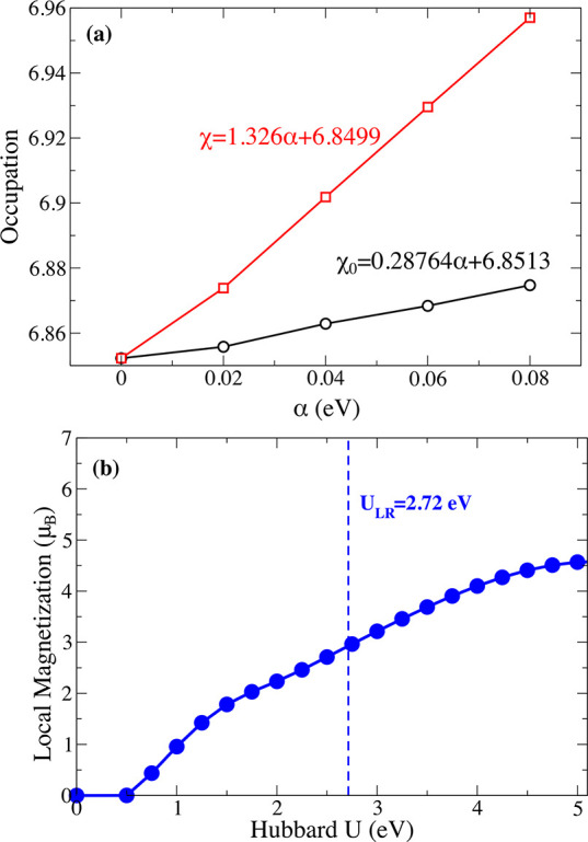
 – χ–1. (b) Variation of the local magnetization
at
the defect antisite versus U. At U = 0, no magnetic moments are observed as the defect shows a symmetric
configuration at the Mo–Mo bonds. At U >
0.5
eV, this symmetry is broken and the defect develops an appreciable
magnetic moment that increases with U as a result
of the increased localization of the bands. All panels are adapted
with permission under a Creative Common CC BY-NC license from ref (382). Copyright 2019 AAAS.
– χ–1. (b) Variation of the local magnetization
at
the defect antisite versus U. At U = 0, no magnetic moments are observed as the defect shows a symmetric
configuration at the Mo–Mo bonds. At U >
0.5
eV, this symmetry is broken and the defect develops an appreciable
magnetic moment that increases with U as a result
of the increased localization of the bands. All panels are adapted
with permission under a Creative Common CC BY-NC license from ref (382). Copyright 2019 AAAS.
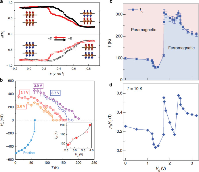
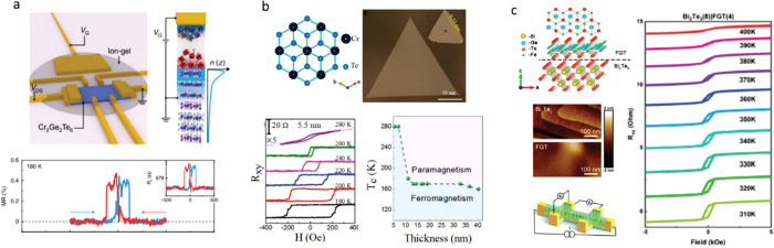
 of multilayer CGT as a function of temperature
at different gate voltages and in the pristine case. Inset: The dependence
of TC on gate voltage. Adapted with permission from ref (86). Copyright 2020 Springer
Nature. (c) TC of a trilayer
FGT as a function of gate voltage. (d) HC of a trilayer FGT as a function
of gate voltage at 10 K. Panels (c) and
(d) are adapted with permission from ref (12). Copyright 2018 Springer Nature.
of multilayer CGT as a function of temperature
at different gate voltages and in the pristine case. Inset: The dependence
of TC on gate voltage. Adapted with permission from ref (86). Copyright 2020 Springer
Nature. (c) TC of a trilayer
FGT as a function of gate voltage. (d) HC of a trilayer FGT as a function
of gate voltage at 10 K. Panels (c) and
(d) are adapted with permission from ref (12). Copyright 2018 Springer Nature.
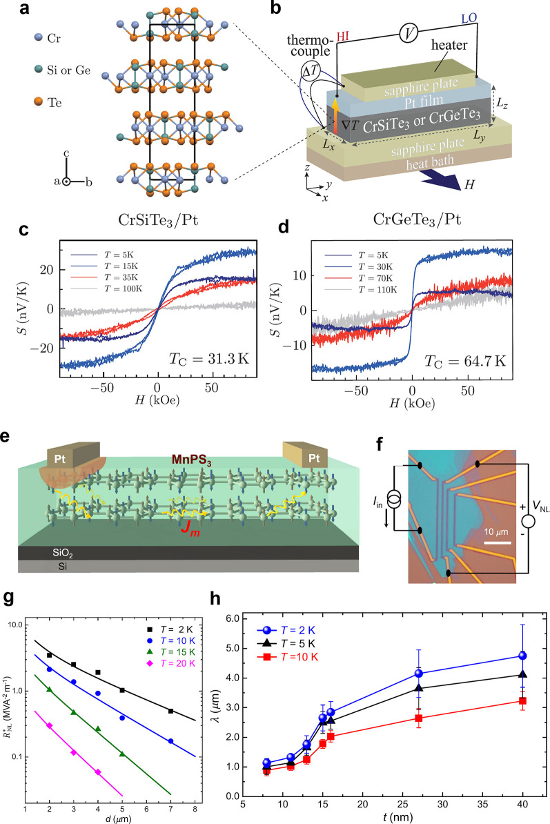
 as a function of distance (d)
for selected temperatures in a 16 nm-thick MnPS3 flake.
The solid lines represent the best-fitting results based on a diffusion
equation. (h) Magnon diffusion length
as a function of MnPS3 thickness (t) for
selected temperatures. Panels (e–h)
are adapted with permission under a Creative Commons CC BY 4.0 license
from ref (468). Copyright
2019 American Physical Society.
as a function of distance (d)
for selected temperatures in a 16 nm-thick MnPS3 flake.
The solid lines represent the best-fitting results based on a diffusion
equation. (h) Magnon diffusion length
as a function of MnPS3 thickness (t) for
selected temperatures. Panels (e–h)
are adapted with permission under a Creative Commons CC BY 4.0 license
from ref (468). Copyright
2019 American Physical Society.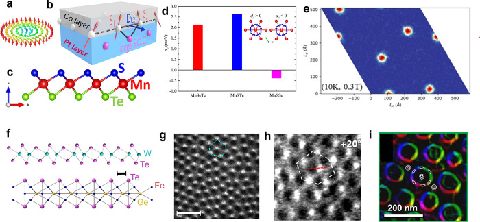
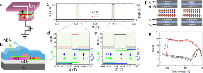
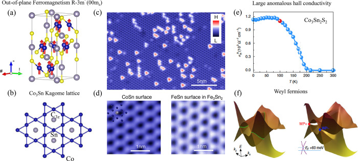
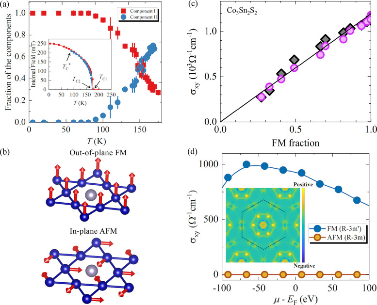
 , below which only FM component is observed.
(b) Spin structures of Co3Sn2S2, i.e., the FM and the in-plane AF (or AFM) structures. (c)
The correlation plot of anomalous hall conductivity versus FM fraction.
(d) Calculated AHC for out-of-plane FM and in-plane AF structures.
The inset shows the calculated Berry curvature distribution in the
BZ at the FM phase. All panels are adapted with permission under a
Creative Commons CC BY 4.0 license from ref (514). Copyright 2020 Springer
Nature.
, below which only FM component is observed.
(b) Spin structures of Co3Sn2S2, i.e., the FM and the in-plane AF (or AFM) structures. (c)
The correlation plot of anomalous hall conductivity versus FM fraction.
(d) Calculated AHC for out-of-plane FM and in-plane AF structures.
The inset shows the calculated Berry curvature distribution in the
BZ at the FM phase. All panels are adapted with permission under a
Creative Commons CC BY 4.0 license from ref (514). Copyright 2020 Springer
Nature.
References
-
- Lin M.-W.; Zhuang H. L.; Yan J.; Ward T. Z.; Puretzky A. A.; Rouleau C. M.; Gai Z.; Liang L.; Meunier V.; Sumpter B. G.; Ganesh P.; Kent P. R. C.; Geohegan D. B.; Mandrus D. G.; Xiao K. Ultrathin Nanosheets of CrSiTe3: A Semiconducting Two-Dimensional Ferromagnetic Material. J. Mater. Chem. C 2016, 4, 315–322. 10.1039/C5TC03463A. - DOI
-
- Lee S.; Choi K.-Y.; Lee S.; Park B. H.; Park J.-G. Tunneling Transport of Mono- and Few-Layers Magnetic van der Waals MnPS3. APL Mater. 2016, 4, 086108. 10.1063/1.4961211. - DOI
-
- Huang B.; Clark G.; Navarro-Moratalla E.; Klein D. R.; Cheng R.; Seyler K. L.; Zhong D.; Schmidgall E.; McGuire M. A.; Cobden D. H.; Yao W.; Xiao D.; Jarillo-Herrero P.; Xu X. Layer-Dependent Ferromagnetism in a van der Waals Crystal Down to the Monolayer Limit. Nature 2017, 546, 270–273. 10.1038/nature22391. - DOI - PubMed
