

Artificial intelligence deep learning for 3D IC reliability prediction
- PMID: 35468910
- PMCID: PMC9035975
- DOI: 10.1038/s41598-022-08179-z
Artificial intelligence deep learning for 3D IC reliability prediction
Abstract
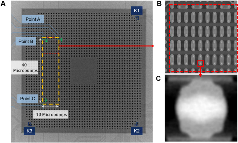
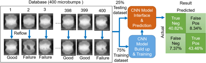
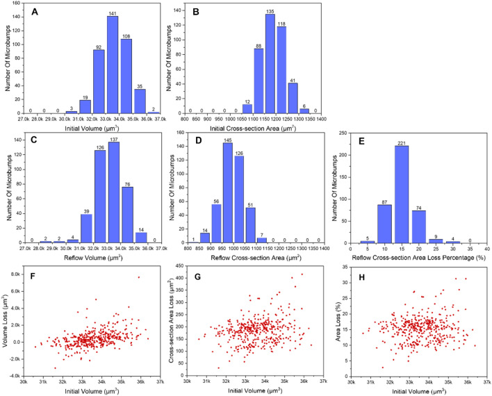
Three-dimensional integrated circuit (3D IC) technologies have been receiving much attention recently due to the near-ending of Moore's law of minimization in 2D IC. However, the reliability of 3D IC, which is greatly influenced by voids and failure in interconnects during the fabrication processes, typically requires slow testing and relies on human's judgement. Thus, the growing demand for 3D IC has generated considerable attention on the importance of reliability analysis and failure prediction. This research conducts 3D X-ray tomographic images combining with AI deep learning based on a convolutional neural network (CNN) for non-destructive analysis of solder interconnects. By training the AI machine using a reliable database of collected images, the AI can quickly detect and predict the interconnect operational faults of solder joints with an accuracy of up to 89.9% based on non-destructive 3D X-ray tomographic images. The important features which determine the "Good" or "Failure" condition for a reflowed microbump, such as area loss percentage at the middle cross-section, are also revealed.
© 2022. The Author(s).
Conflict of interest statement
The authors declare no competing interests.
Figures

References
-
- Tu KN. Reliability challenges in 3D IC packaging technology. Microelectron. Reliab. 2011;51:517–523. doi: 10.1016/j.microrel.2010.09.031. - DOI
-
- Tu KN, Gusak AM. A unified model of mean-time-to-failure for electromigration, thermomigration, and stress-migration based on entropy production. J. Appl. Phys. 2019;126:075109. doi: 10.1063/1.5111159. - DOI
-
- Martins, A. et al. In 2018 International Wafer Level Packaging Conference (IWLPC) 1–6.
