Electron beam lithography for direct patterning of MoS2 on PDMS substrates
- PMID: 35479206
- PMCID: PMC9033649
- DOI: 10.1039/d1ra00885d
Electron beam lithography for direct patterning of MoS2 on PDMS substrates
Abstract
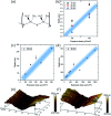
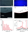
Precise patterning of 2D materials into micro- and nanostructures presents a considerable challenge and many efforts are dedicated to the development of processes alternative to the standard lithography. In this work we show a fabrication technique based on direct electron beam lithography (EBL) on MoS2 on polydimethylsiloxane (PDMS) substrates. This easy and fast method takes advantage of the interaction of the electron beam with the PDMS, which at high enough doses leads to cross-linking and shrinking of the polymer. At the same time, the adhesion of MoS2 to PDMS is enhanced in the exposed regions. The EBL acceleration voltages and doses are optimized in order to fabricate well-defined microstructures, which can be subsequently transferred to either a flexible or a rigid substrate, to obtain the negative of the exposed image. The reported procedure greatly simplifies the fabrication process and reduces the number of steps compared to standard lithography and etching. As no additional polymer, such as polymethyl methacrylate (PMMA) or photoresists, are used during the whole process the resulting samples are free of residues.
This journal is © The Royal Society of Chemistry.
Conflict of interest statement
There are no conflicts of interest to declare.
Figures


References
-
- Choi W. Choudhary N. Han G. H. Park J. Akinwande D. Lee Y. H. Mater. Today. 2017;20:116. doi: 10.1016/j.mattod.2016.10.002. - DOI
-
- Hallam T. Berner N. C. Yim C. Duesberg G. S. Adv. Mater. Interfaces. 2014;1:1400115. doi: 10.1002/admi.201400115. - DOI
-
- Gammelgaard L. Caridad J. M. Cagliani A. Mackenzie D. M. A. Petersen D. H. Booth T. J. Bøggild P. 2D Mater. 2014;1:035005. doi: 10.1088/2053-1583/1/3/035005. - DOI
LinkOut - more resources
Full Text Sources
Research Materials

