Review
. 2021 Aug 17;11(45):27897-27924.
doi: 10.1039/d1ra04876g. eCollection 2021 Aug 16.

A review on the use of DFT for the prediction of the properties of nanomaterials

Affiliations
Review

A review on the use of DFT for the prediction of the properties of nanomaterials

Priyanka Makkar et al. RSC Adv. .

Abstract

Nanostructured materials have gained immense attraction because of their extraordinary properties compared to the bulk materials to be used in a plethora of applications in myriad fields. In this review article, we have discussed how the Density Functional Theory (DFT) calculation can be used to explain some of the properties of nanomaterials. With some specific examples here, it has been shown that how closely the different properties of nanomaterials (such as optical, optoelectronics, catalytic and magnetic) predicted by DFT calculations match well with the experimentally determined values. Some examples were discussed in detail to inspire the experimental scientists to conduct DFT-based calculations along with the experiments to derive a better understanding of the experimentally obtained results as well as to predict the properties of the nanomaterial. We have pointed out the challenges associated with DFT, and potential future perspectives of this new exciting field.


Conflict of interest statement

The authors declare no conflict of interest.

Figures

Fig. 1
Fig. 1. (a) Schematic representation of the quantum confinement effects: the bandgap (or HOMO–LUMO gap) of the semiconductor nanocrystal increases with decreasing size, while discrete energy levels arise at the band-edges. The energy separation between the band-edge levels also increases with decreasing size. (b) Photograph of five colloidal dispersions of CdSe QDs with different sizes, under excitation with a UV-lamp in the dark. The color of the photoluminescence changes from red to blue as the QD diameter is reduced from 6 to 2 nm. This figure has been reproduced from ref. with permission from Springer Nature, copyright 2016.
Fig. 2
Fig. 2. Calculated absorption spectra for silver nanorods (Ag19, Ag25, Ag31, Ag37, Ag43, Ag49, Ag55, and Ag67) at the (a) TD-DFT and (b) TD-DFTB levels of theory. This figure is reproduced from ref. with permission from the American Chemical Society, copyright 2018.
Fig. 3
Fig. 3. Size comparisons of optical absorption spectra for octahedral (a), truncated octahedral (b), and icosahedral (c) gold nanoparticles using the LB94 functional. This figure is reproduced from ref. with permission from the American Chemical Society, copyright 2015.
Fig. 4
Fig. 4. Calculated energy band structure using different XC functionals: (a) LDA with red circle showing the underestimated band gap, reproduced with permission, copyright 1995 American Physical Society; (b) GGA and GGA+U, and (c) the enlarged energy gap. This figure is reproduced from ref. with permission from American Chemical Society, copyright 2013.
Fig. 5
Fig. 5. Calculated energy band structure of synthesized ZnO using different functionals: (a) LDA, GGA-PBE, and GGA-PBE Sol and (b) LDA+U, GGA-PBE+U, and GGA-PBESol+U. This figure is reproduced from ref. with permission from IOPscience, copyright 2017.
Fig. 6
Fig. 6. Electronic band structures of (A) superlattices, (B) BiFeO3 superlattices for spin up, (C) BiFeO3 superlattices for spin down, (D) BiFeO3–graphene superlattices for spin-up, and (E) BiFeO3–graphene superlattices for spin-down. This figure is reproduced from ref. with permission from the American Chemical Society, copyright 2017.
Fig. 7
Fig. 7. Projected density of states of (A) graphene, (B) BiFeO3, and (C) BFO–graphene superlattices. The Fermi level is referenced to zero energy, as indicated by the dotted line. This figure is reproduced from ref. with permission from the American Chemical Society, copyright 2017.
Fig. 8
Fig. 8. (A) Electronic total charge density and (B) difference charge density plots of the BFO–graphene composite interface. This figure is reproduced from ref. with permission from the American Chemical Society, copyright 2017.
Fig. 9
Fig. 9. (a) Mixing energy versus atomic composition for 79-atom Au–Rh nanoalloy TO clusters and monometallic counterparts. The most stable cluster (Rh19@Au60) is enlarged in inset. (b) Structure and corresponding adsorption energy for clusters of selected compositions adsorbed on TiO2(110). Blue, yellow, cyan, and red spheres represent Rh, Au, Ti, and O atoms, respectively. Only one layer of the TiO2 slab is shown for simplicity. (c) Schematic view of the energetics of free and supported Au50Rh29 clusters. This figure is reproduced from ref. with permission from Scientific Reports, copyright 2016.
Fig. 10
Fig. 10. DFT-simulated 4-NP on the surface of (a) Au NPs, (b) Au–Cu NPs, (c) Au/rGO, and (d) Au–Cu/rGO. This figure is reproduced from ref. with permission from Elsevier, copyright 2017.
Fig. 11
Fig. 11. The band structure and density of states of Co–Ni interface. This figure is reproduced from ref. with permission from the American Chemical Society, copyright 2019.
Fig. 12
Fig. 12. The band structure and density of states of Co–Ni–graphene superlattice. This figure is reproduced from ref. with permission from American Chemical Society, copyright 2019.
Fig. 13
Fig. 13. Charge density plots of the (a) Co–Ni interface and (b) Co–Ni graphene interface and difference charge density plot of the (c) Co–Ni interface and (d) Co–Ni graphene interface (where the red color represents charge accumulation and the blue color represents charge depletion in the difference charge density plot). This figure is reproduced from ref. with permission from the American Chemical Society, copyright 2019.
Fig. 14
Fig. 14. (a) Electrochemical impedance spectra of the synthesized materials, and the insets show the high-frequency region and equivalent circuit used for the fitting of the Nyquist plot. (b) |Z| versus frequency plot, (c) phase angle versus frequency plots. This figure is reproduced from ref. with permission from the American Chemical Society, copyright 2019.
Fig. 15
Fig. 15. The band structure and density of states of Ag–Ni interface spin up. This figure is reproduced from ref. with permission from the Royal Society of Chemistry, copyright 2018.
Fig. 16
Fig. 16. The band structure and density of states of Ag–Ni interface spin down. This figure is reproduced from ref. with permission from Royal Society of Chemistry, copyright 2018.
Fig. 17
Fig. 17. The band structure and density of states of Ag–Ni–graphene superlattice spin down. This figure is reproduced from ref. with permission from the Royal Society of Chemistry, copyright 2018.
Fig. 18
Fig. 18. Electronic total charge density plot of (a) graphene, (b) Ni slab, (c) Ag slab, (d) Ag–Ni interface, (e) Ag–Ni–graphene superlattice, difference charge density plots of (f) Ag–Ni interface, and (g) Ag–Ni–graphene superlattice where red color represents charge accumulation and blue color represents charge depletion in difference charge density plot. This figure is reproduced from ref. with permission from American Chemical Society, copyright 2018.
Fig. 19
Fig. 19. Electron deformation density of the 2 × 2 layer of Pt (111) and Ag (111) surfaces, and the loss and gain of electrons are indicated in blue and red, respectively. This figure is reproduced from ref. with permission from Elsevier, copyright 2017.
Fig. 20
Fig. 20. The TDOS and partial density of states (PDOS) of Ag (a), Ag@Pt (b) and Pt (c) nanoparticles, the s-electron PDOS of Ag cores (d) and the d-electron PDOS of Pt shells (e), respectively. This figure is reproduced from ref. with permission from Elsevier, copyright 2017.
Fig. 21
Fig. 21. The cluster models of Ti10O32H24 (A) and Ti13O43H34 (B) were used to mimic rutile TiO2(110) as well as to estimate the formation energy of different oxygen vacancy sites. The first model A is a completely symmetrical one (with a relatively small number of structural parameters for the geometry optimization), while the second model B is a slightly extended form involving additional bulk as well as Ti5C centers. The dark blue and grey balls stand for the selected precursor bridging O center on which the vacancy would be formed and the Ti5C center, respectively. This figure is reproduced from ref. with permission from the American Chemical Society, copyright 2007.
Fig. 22
Fig. 22. Potential energy diagram for the epoxide and acetaldehyde formation from ethylene and atomic oxygen adsorbed on a Au (111) surface (black line) and nanoparticle (blue line). This figure is reproduced from ref. with permission from the American Chemical Society, copyright 2010.
Fig. 23
Fig. 23. Isodensity surfaces (0.03 e bohr−3) of the key molecular orbitals of TinO2n+2H4 clusters (n = 14, 24, 54, from left to right, respectively), calculated by DFT at the B3LYP/LANL2DZ level in a water solvent. The first two rows display the top and a perspective view of the LUMOs, whereas the bottom two rows show the top and a perspective view of the HOMOs. Atom colors: Ti, grey; O, red; and H, light grey. This figure is reproduced from ref. with permission from MDPI, copyright 2019.
Fig. 24
Fig. 24. (A) The active sites of BPA for OPCN attacks. DFT calculated structures of reactants, intermediates, and transition state for the degradation of BPA attacked by OPCN catalysts with (B) N atoms or (C) doped O atoms as reactive sites white, red, gray and blue balls represented H, O, C and N elements, respectively. This figure is reproduced from ref. with permission from Elsevier, copyright 2019.
Fig. 25
Fig. 25. (a) Spin polarized total valence electron charge density, n(r) over the graphene plane in units of e Å−3 for (a) and (b) pristine, (c) and (d) Cr-doped and (e) and (f) Mo-doped graphene. This figure is reproduced from ref. with permission from Elsevier, copyright 2016.
Fig. 26
Fig. 26. A comparison of the spin-polarized density of states (DOS) of ideal pristine and doped graphene supercells. The Fermi level set to zero is indicated as the vertical dashed line. This figure is reproduced from ref. with permission from Elsevier copyright, 2020.
Fig. 27
Fig. 27. A comparison of the spin-polarized density of states computed in DFT (colored background areas) and DFT+U approach (solid lines). The Fermi level set to zero is marked as the vertical dashed line. This figure is reproduced from ref. with permission from Elsevier, copyright 2020.
Fig. 28
Fig. 28. Different magnetic configuration considered (a) ferromagnetic (FM), antiferromagnetic (b) A-type, (c) C-type and (d) G-type. Fe (gold), La (green), and O (red). This figure is reproduced from ref. with permission from Elsevier, copyright 2020.
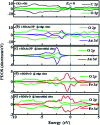
Fig. 29
Fig. 29. Partial density of states (PDOS) showing contribution from C, Au, Fe, and O orbitals in (a) r-GO, (b) r-GO:Au at edge sites, (c) r-GO:Au at interstitial sites, (d) r-GO:Fe–O at edge sites and (e) r-GO:Fe–O at interstitial sites [minimal contributing orbitals to the PDOS are C 2s, O 2s, Au 4s and Fe 2p (not shown)]. This figure is reproduced from ref. with permission from Elsevier, copyright 2020.

Similar articles

Cited by

References

    1. Rabouw F. T. and de Mello Donega C., Handbook of Photoactive Semiconductor Nanocrystal Quantum Dots, Springer, 2017, pp. 1–30
    1. Bora T. Dousse A. Sharma K. Sarma K. Baev A. Hornyak G. L. Dasgupta G. Int. J. Smart Nano Mater. 2018;10:116–143. doi: 10.1080/19475411.2018.1541935. - DOI
    1. Demir H. Grabow L. C. ACS Appl. Nano Mater. 2020;3:6127–6130. doi: 10.1021/acsanm.0c01396. - DOI
    1. Segall M. Lindan P. J. Probert M. J. Pickard C. J. Hasnip P. J. Clark S. Payne M. J. Phys.: Condens. Matter. 2002;14:2717–2744. doi: 10.1088/0953-8984/14/11/301. - DOI
    1. Harun K. Salleh N. A. Deghfel B. Yaakob M. K. Mohamad A. A. Results Phys. 2020;16:102829–102840. doi: 10.1016/j.rinp.2019.102829. - DOI