

Hybrid microchannel-solid state micropore device for fast and optical cell detection
- PMID: 35498312
- PMCID: PMC9049143
- DOI: 10.1039/c9ra09939e
Hybrid microchannel-solid state micropore device for fast and optical cell detection
Abstract
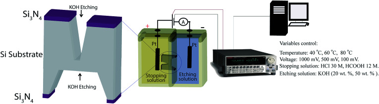
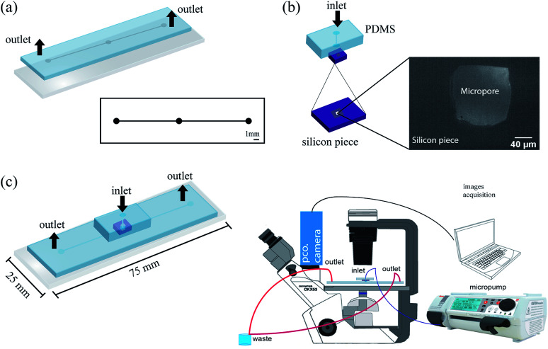
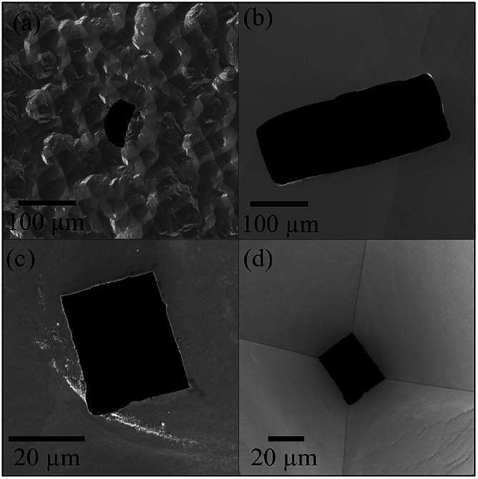
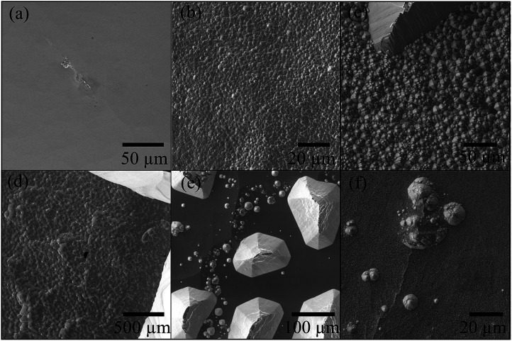
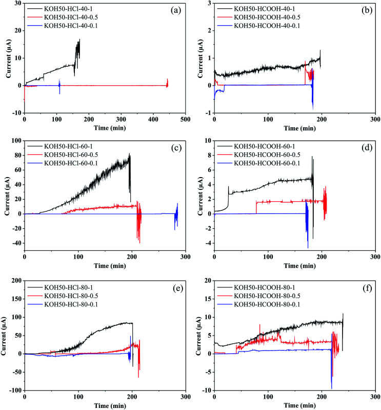
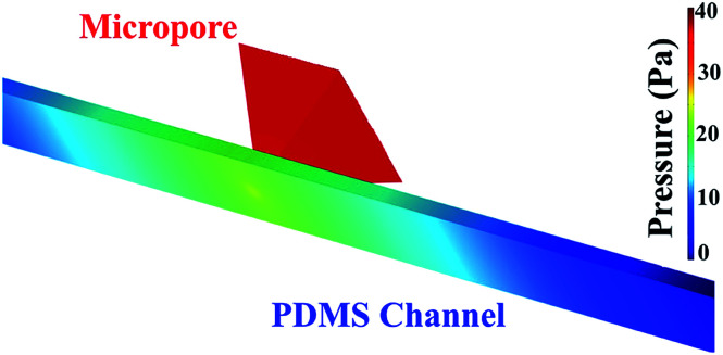
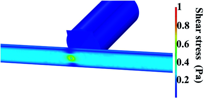
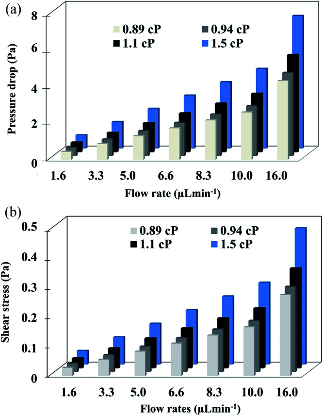
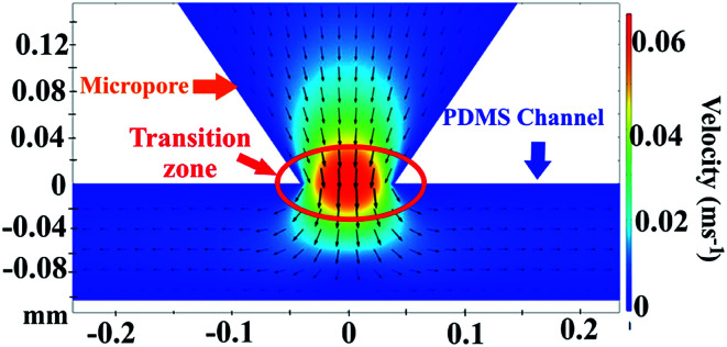
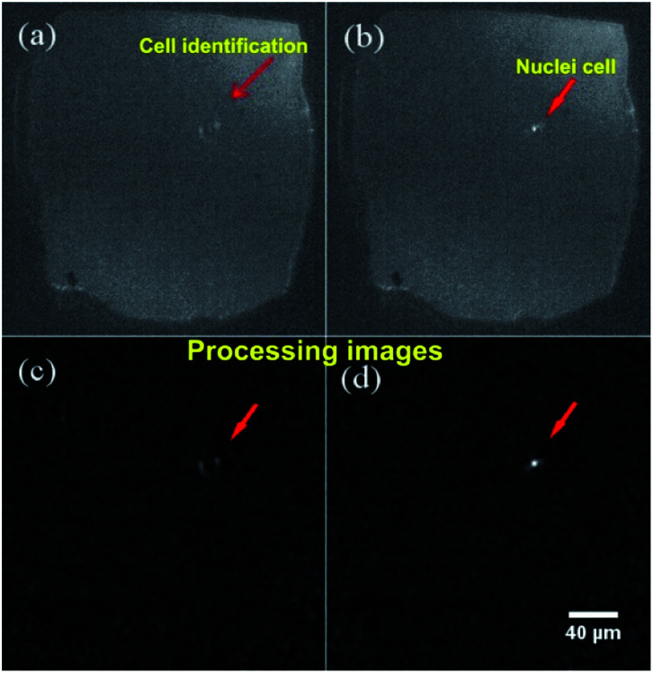
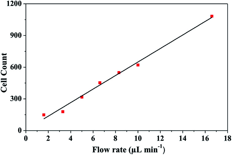
This paper presents a methodology for cell detection and counting using a device that combines PDMS (polydimethylsiloxane) microfluidic multilayer channels with a single solid state micropore. Optimal conditions of solid-state micropore fabrication from crystalline silicon wafers are presented. Micropores of varying size can be obtained by directly etching using an etchant agent concentration of 50 wt% KOH, at varying temperatures (40, 60, 80 °C) and voltages (100, 500, 1000 mV). Scanning Electron Microscopy (SEM), and profilometry techniques have been used for the micropore characterization. In order to find optimal conditions for cell detection a COMSOL Multiphysics simulation was performed. Pressure drop, shear stress, fluid viscosities and flow rates parameters were evaluated. The potential viability of the device for cell detection and counting, avoiding cellular damage, is demonstrated.
This journal is © The Royal Society of Chemistry.
Conflict of interest statement
There are no conflicts to declare.
Figures
Similar articles
-
Fabrication of multilayer-PDMS based microfluidic device for bio-particles concentration detection.Biomed Mater Eng. 2014;24(6):1951-8. doi: 10.3233/BME-141004. Biomed Mater Eng. 2014. PMID: 25226891
-
The Deformation of Polydimethylsiloxane (PDMS) Microfluidic Channels Filled with Embedded Circular Obstacles under Certain Circumstances.Molecules. 2016 Jun 18;21(6):798. doi: 10.3390/molecules21060798. Molecules. 2016. PMID: 27322239 Free PMC article.
-
Cost-effective fabrication of photopolymer molds with multi-level microstructures for PDMS microfluidic device manufacture.RSC Adv. 2020 Jan 23;10(7):4071-4079. doi: 10.1039/c9ra07955f. eCollection 2020 Jan 22. RSC Adv. 2020. PMID: 35492655 Free PMC article.
-
Microfluidic Liquid Cell with Silicon Nitride Super-Thin Membrane for Electron Microscopy of Samples in Liquid.Biosensors (Basel). 2022 Dec 7;12(12):1138. doi: 10.3390/bios12121138. Biosensors (Basel). 2022. PMID: 36551105 Free PMC article.
-
Gaining Micropattern Fidelity in an NOA81 Microsieve Laser Ablation Process.Micromachines (Basel). 2020 Dec 27;12(1):21. doi: 10.3390/mi12010021. Micromachines (Basel). 2020. PMID: 33375445 Free PMC article.
Cited by
-
Particle Counting Methods Based on Microfluidic Devices.Micromachines (Basel). 2023 Sep 1;14(9):1722. doi: 10.3390/mi14091722. Micromachines (Basel). 2023. PMID: 37763885 Free PMC article. Review.
-
GEMA-An Automatic Segmentation Method for Real-Time Analysis of Mammalian Cell Growth in Microfluidic Devices.J Imaging. 2022 Oct 14;8(10):281. doi: 10.3390/jimaging8100281. J Imaging. 2022. PMID: 36286375 Free PMC article.
-
BSEO-Semiautomatic Method for Determination of Oil Recovery with Nanofluids in Microfluidic Devices.ACS Omega. 2024 May 9;9(20):22031-22042. doi: 10.1021/acsomega.4c00040. eCollection 2024 May 21. ACS Omega. 2024. PMID: 38799315 Free PMC article.
-
Using novel micropore technology combined with artificial intelligence to differentiate Staphylococcus aureus and Staphylococcus epidermidis.Sci Rep. 2024 Mar 24;14(1):6994. doi: 10.1038/s41598-024-55773-4. Sci Rep. 2024. PMID: 38523156 Free PMC article.
-
Photopolymer Flexographic Printing Plate Mold for PDMS Microfluidic Manufacture.Polymers (Basel). 2025 Jun 20;17(13):1723. doi: 10.3390/polym17131723. Polymers (Basel). 2025. PMID: 40647734 Free PMC article. Review.
References
LinkOut - more resources
Full Text Sources