. 2022 May 4;13(1):2431.
doi: 10.1038/s41467-022-29990-2.

Superconducting spintronic tunnel diode

Affiliations

Superconducting spintronic tunnel diode

E Strambini et al. Nat Commun. .

Abstract

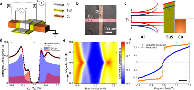
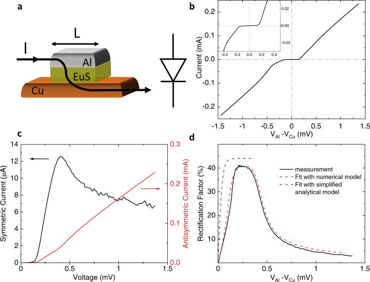
Diodes are key elements for electronics, optics, and detection. Their evolution towards low dissipation electronics has seen the hybridization with superconductors and the realization of supercurrent diodes with zero resistance in only one direction. Here, we present the quasi-particle counterpart, a superconducting tunnel diode with zero conductance in only one direction. The direction-selective propagation of the charge has been obtained through the broken electron-hole symmetry induced by the spin selection of the ferromagnetic tunnel barrier: a EuS thin film separating a superconducting Al and a normal metal Cu layer. The Cu/EuS/Al tunnel junction achieves a large rectification (up to ∼40%) already for a small voltage bias (∼200 μV) thanks to the small energy scale of the system: the Al superconducting gap. With the help of an analytical theoretical model we can link the maximum rectification to the spin polarization (P) of the barrier and describe the quasi-ideal Shockley-diode behavior of the junction. This cryogenic spintronic rectifier is promising for the application in highly-sensitive radiation detection for which two different configurations are evaluated. In addition, the superconducting diode may pave the way for future low-dissipation and fast superconducting electronics.


Conflict of interest statement

With the Institute Nanoscienze-CNR, the following authors: E.S., M.S., F.G., P.V., T.T.H., S.I, and F.S.B., have filed a patent (International Application N. PCT/IT2021/000038 “APPARATUS AND METHOD FOR SUPERCONDUCTING DIODE”, status: pending, aspect of manuscript covered in patent application: rectification and diode-behavior of the material combinations, architecture and measurement configurations presented). The remaining authors declare no competing interests.

Figures

Fig. 1
Fig. 1. Working principle and characteristics of the superconducting tunnel diode.
a Schematic of the device structure: a Cu strip (orange) is covered by a EuS layer (green) and a perpendicular Al strip (gray). Measurement setups: The electric current is applied (i) from the Al to the Cu strip or (ii) along the Cu strip. The voltage drop is measured between the Al and the Cu strip on the remaining two wires of the four-wire set-up. b Visible light microscopy image of the device. c Schematic of the DoS along the vertical axis of the structure (Al/EuS/Cu from top to bottom). The dashed line indicates the Fermi level. Note that the EuS layer induces spin splitting in the superconducting DoS, and spin filtering thanks to the different heights of the tunnel barrier for the two spin species. The red (blue) line corresponds to the spin up (down) DoS in the Al layer. d Exemplary differential conductance (black) measured as a function of voltage across the junction at an applied external magnetic field B of 0.1 T at ≃ 100 mK. By employing a numerical model (detailed in the Methods section, Eqs. (3) and (14)), the fit for the differential conductance (red) and the contributions of the spin up (light blue) and spin down (light red) electrons were calculated with these fitting parameters: Δ0 = 0.33meV, h = 0.32Δ0, P = 0.48, Γ = 0.01Δ0, T = 300 mK. e Color map of the differential conductance dI/dV(V) measured for B ranging from −0.2 T to 0.2 T. The sweep direction is indicated by the arrow. The data in panel d corresponds to the dash-dotted line (B = 0.1 T). The coercive field at the temperature of this measurement (100 mK) corresponds to −9 mT, indicated by a dashed line. f Exchange field (h) induced in the superconducting Al strip (blue) and polarization (P) of the EuS tunnel barrier as a function of the external magnetic field B. Both quantities are extracted from the best fitting results of the data as shown in panel d. The sweep direction is again indicated by an arrow.
Fig. 2
Fig. 2. Rectification of the superconducting tunnel diode.
a Schematic of the N/FI/S tunnel junction. The path of the tunneling current is indicated by the black line and its arrows. In terms of electronic circuit elements this junction behaves like the indicated diode: the current flows preferentially from the Al layer to the Cu layer while the reverse flow is inhibited. b Current-to-Voltage (I(V)) characteristics of the junction measured at T ≃ 50 mK, B = 0.1 T in the four-wire configuration (i). c Symmetric and antisymmetric parts of the I(V) characteristic of panel c showing a sizable symmetric component of the current. d Rectification coefficient R(V) = ISym(V)/IAntisym(V) evaluated from e (black line) along with the comparison with the rectification extracted from the approximated analytical model R=Ptanh[eV/(2KBT)] (blue line) and the full numerical ones (red line). Details of the numerical model can be found in the Methods section, specifically in Eqs. (3) and (14). Notice the good qualitative agreement with the simplified model predicting the saturation at R ≃ P ∼ 40% at 225–280 μV. The model ceases to work when eV ≳ Δ − h ∼ 250 μeV. The discrepancy between the analytical model and the experiment mostly comes from weak inelastic scattering, and to a lesser extent from spin relaxation and orbital depairing.
Fig. 3
Fig. 3. Transverse rectification of the superconducting tunnel diode.
a Schematic of the N/FI/S tunnel junction and current path. A biasing current IH is applied from one end of the Cu strip to the other, while the voltage drop across the junction is measured from the Al contact to the Cu one. The path of tunneling current is indicated by the black line and its arrows. b Electronic circuit diagram of the setup. Note that the EuS layer effectively acts as a twofold rectifier for the distributed incoming and outgoing currents tunneling through the FI barrier. c Transverse voltage drop Vsym(ICu) measured across the barrier as a function of the applied current IH at different B and at 50 mK. Note that even at zero applied magnetic field (orange curve) a voltage drop occurs, while at the coercive field (B ≃ − 14 mT) the signal is zero due to the non-polarization of the EuS layer. The V(I) was symmetrized in order to discard the Ohmic (linear) component originating from the N lead. In the inset, the Vsym measured at 0.2 T is compared with the calculated data points obtained through a theoretical model of the circuit and using the rectification value obtained from the experimental data.
Fig. 4
Fig. 4. Temperature dependence of the superconducting rectifier.
a Differential conductance vs. voltage of the junction measured for different temperatures from 50 mK to 1.9 K. b Temperature evolution of the transverse rectification voltage vs. biasing current. Both measurements are performed at B = 0.1 T.

References

    1. Braginski AI. Superconductor electronics: status and outlook. J. Supercond. Nov. Magn. 2019;32:23–44. doi: 10.1007/s10948-018-4884-4. - DOI
    1. Farrah D, et al. Review: far-infrared instrumentation and technological development for the next decade. JATIS. 2019;5:020901.
    1. Ono K, Austing D, Tokura Y, Tarucha S. Current rectification by pauli exclusion in a weakly coupled double quantum dot system. Science. 2002;297:1313–1317. doi: 10.1126/science.1070958. - DOI - PubMed
    1. DiCarlo L, Marcus C, Harris Jr J. Photocurrent, rectification, and magnetic field symmetry of induced current through quantum dots. Phys. Rev. Lett. 2003;91:246804. doi: 10.1103/PhysRevLett.91.246804. - DOI - PubMed
    1. Ando F, et al. Observation of superconducting diode effect. Nature. 2020;584:373–376. doi: 10.1038/s41586-020-2590-4. - DOI - PubMed