Review
. 2020 Aug 19;10(51):30529-30602.
doi: 10.1039/d0ra03183f. eCollection 2020 Aug 17.

A review of molybdenum disulfide (MoS2) based photodetectors: from ultra-broadband, self-powered to flexible devices

Affiliations
Review

A review of molybdenum disulfide (MoS2) based photodetectors: from ultra-broadband, self-powered to flexible devices

Hari Singh Nalwa. RSC Adv. .

Abstract

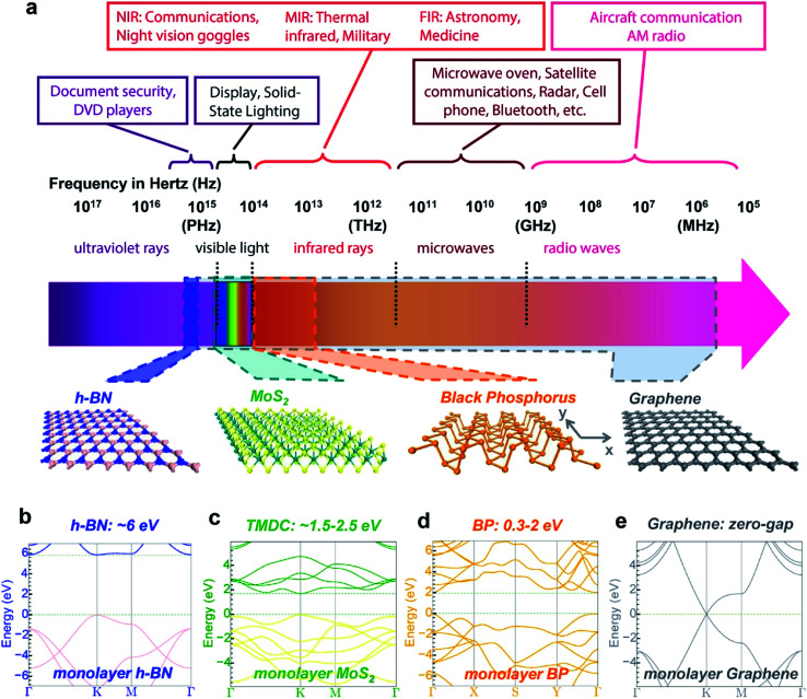
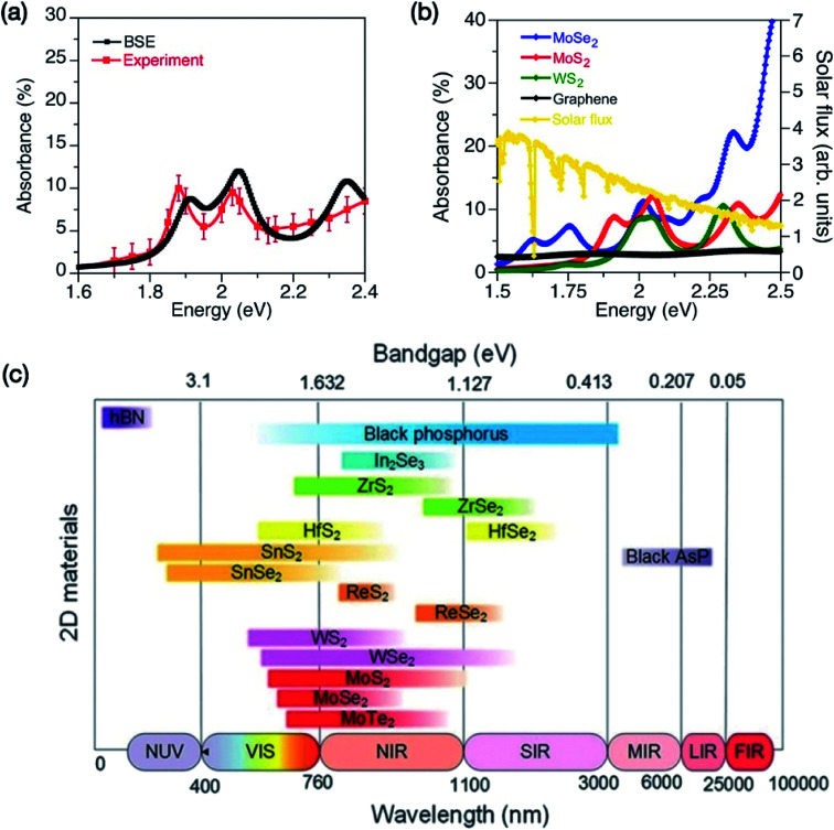
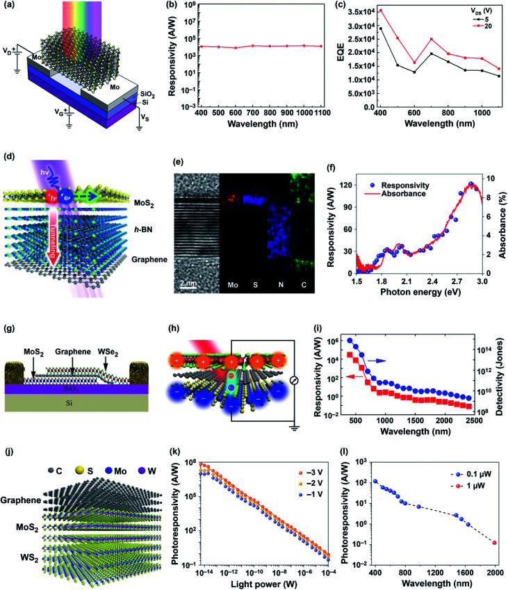
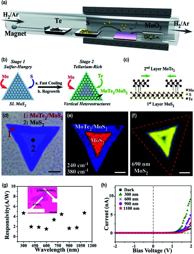
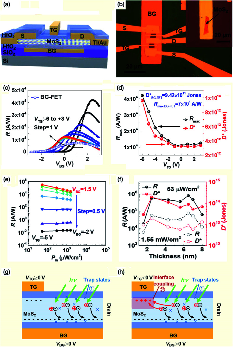
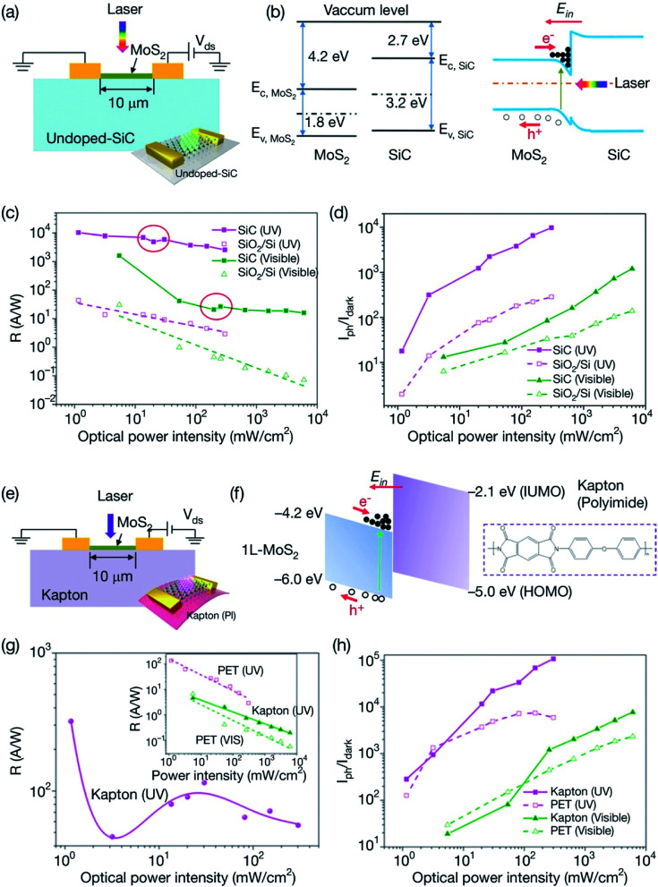
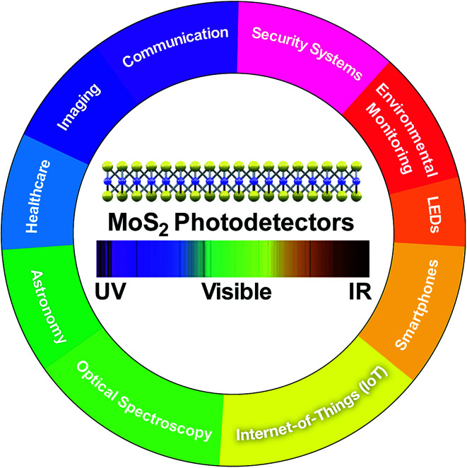
Two-dimensional transition metal dichalcogenides (2D TMDs) have attracted much attention in the field of optoelectronics due to their tunable bandgaps, strong interaction with light and tremendous capability for developing diverse van der Waals heterostructures (vdWHs) with other materials. Molybdenum disulfide (MoS2) atomic layers which exhibit high carrier mobility and optical transparency are very suitable for developing ultra-broadband photodetectors to be used from surveillance and healthcare to optical communication. This review provides a brief introduction to TMD-based photodetectors, exclusively focused on MoS2-based photodetectors. The current research advances show that the photoresponse of atomic layered MoS2 can be significantly improved by boosting its charge carrier mobility and incident light absorption via forming MoS2 based plasmonic nanostructures, halide perovskites-MoS2 heterostructures, 2D-0D MoS2/quantum dots (QDs) and 2D-2D MoS2 hybrid vdWHs, chemical doping, and surface functionalization of MoS2 atomic layers. By utilizing these different integration strategies, MoS2 hybrid heterostructure-based photodetectors exhibited remarkably high photoresponsivity raging from mA W-1 up to 1010 A W-1, detectivity from 107 to 1015 Jones and a photoresponse time from seconds (s) to nanoseconds (10-9 s), varying by several orders of magnitude from deep-ultraviolet (DUV) to the long-wavelength infrared (LWIR) region. The flexible photodetectors developed from MoS2-based hybrid heterostructures with graphene, carbon nanotubes (CNTs), TMDs, and ZnO are also discussed. In addition, strain-induced and self-powered MoS2 based photodetectors have also been summarized. The factors affecting the figure of merit of a very wide range of MoS2-based photodetectors have been analyzed in terms of their photoresponsivity, detectivity, response speed, and quantum efficiency along with their measurement wavelengths and incident laser power densities. Conclusions and the future direction are also outlined on the development of MoS2 and other 2D TMD-based photodetectors.


Conflict of interest statement

There are no conflicts to declare.

Figures

Fig. 1
Fig. 1. (a) 2D materials covering a very wide range of the electromagnetic spectrum, from the NIR and MIR to the FIR, and their corresponding applications. The bottom section shows the atomic structures of h-BN, MoS2, black phosphorus (BP) and graphene from left to right. The electromagnetic spectral ranges covered by different 2D materials are depicted using colored polygons. (b–e) Band structures and bandgaps of monolayer h-BN (b), MoS2 (c), BP (d) and gapless graphene (e). Reprinted with permission from ref. 90, copyright © 2014 Macmillan Publishers Limited.
Fig. 2
Fig. 2. (a) A comparison of the computed absorbance obtained by Bethe–Salpeter equation (BSE) with experimentally measured absorbance of a MoS2 monolayer. (b) A comparison of the optical absorbance of MoS2, MoSe2, and WS2 monolayers with that of graphene along with the incident AM1.5G solar flux. Reprinted with permission from ref. 116a, copyright © American Chemical Society. (c) Band-gaps of different atomic layered 2D nanomaterials (MoS2, MoSe2, MoTe2, WS2, WSe2, ReS2, ReSe2, SnS2, SnSe2, HfS2, HfSe2, ZrS2, ZrSe2, In2Se3, black AsP, black phosphorus (BP) and h-BN) with their corresponding photodetection range varying from near ultraviolet (NUV) to long infrared (LIR). Reprinted with permission from ref. 116b, copyright © Wiley.
Fig. 3
Fig. 3. (a and b) Schematic illustration of monolayer and bilayer MoS2 on an atomic scale. The blue balls represent Mo atoms, while the yellow balls represent S atoms in MoS2. The direct bandgap of 1.8 eV observed in monolayer (1L) MoS2 transits to the indirect bandgap of 1.6 eV for bilayer (2L) MoS2 and to 1.2 eV for multilayer (ML) MoS2. In a bilayer (2L), MoS2 single layers are bound by van der Waals forces having a nanoscale distance between the adjacent layers. (c) Photoresponsivity of a monolayer MoS2 photodetector measured as a function of illumination wavelength in the 400 nm to 800 nm range. The photodetector shows an increasing photoresponsivity as the illumination wavelength is decreased from 680 nm to 400 nm. The monolayer MoS2-based photodetectors can be used over a broad spectral range. The inset shows the structural view of a monolayer (6.5 Å thick) MoS2 photodetector deposited on a back gate substrate with Au electrodes. Reprinted with permission from ref. 171, copyright © 2013 Macmillan Publishers Limited. (d) Schematic of NaCl-assisted layer-controlled low pressure CVD growth of MoS2 flakes. (e) Layer-dependent Raman spectra of MoS2 flakes showing the variation in the modes with increasing layer thickness. (f) Layer-dependent PL spectra of MoS2 flakes. Reprinted with permission from ref. 174, copyright © American Chemical Society. (g) Photoresponsivity of the MoS2/Si heterojunction photodetector as a function of reverse bias voltage at a 660 nm illumination wavelength under different incident laser powers. (h) Photoresponsivity of the MoS2/Si photodetector as a function of the thickness of MoS2 flakes at a bias voltage of 2.0 V under different incident powers. (i) Detectivity of the MoS2/Si photodetector as a function of the thickness of MoS2 flakes. Reprinted with permission from ref. 175, copyright © American Chemical Society.
Fig. 4
Fig. 4. (a) Schematic illustration of the 3D RGO–MoS2/pyramid Si heterojunction-based photodetector. (b) A comparison of the absorption spectra of planar and pyramid Si, RGO (also referred as rGO), and RGO–MoS2/Si heterojunction devices. (c) Photosensitivity of the RGO–MoS2/pyramid Si heterojunction-based device between 350 to 1100 nm wavelength region. (d and e) Photocurrent switching behavior of heterojunction device measured under light illuminations at 1310 and 1550 nm at zero bias voltage (V = 0), self-powered devices. (f) Photocurrent switching behavior of heterojunction devices measured under 1870, 1940, 2200, 3460 and 4290 nm (NIR–MIR) light illuminations. (g) Photoresponsivity (R) and specific detectivity (D*) curves of the heterojunction device measured as a function of wavelength from 1310 nm to 4290 nm at a fixed laser power intensity of 50 mW under zero bias voltage. (h) R and D* curves of the heterojunction photodetector measured as a function of laser power intensity at 808 nm at the 100 nW laser power under zero bias voltage. (i) A comparison of the photocurrent switching behavior of RGO–MoS2/pyramid Si and RGO–MoS2/planar Si heterojunction devices measured at 808 nm wavelength under 1 μW laser power intensity. (j) A comparison of the photocurrent switching behavior of RGO–MoS2/pyramid Si heterojunction device with RGO/pyramid Si and MoS2/pyramid Si devices measured at 1550 nm wavelength under 10 mW laser power intensity. (k) A comparison of the wavelength coverage by the RGO–MoS2/pyramid Si heterojunction-based photodetector along with other traditional semiconductor-based photodetectors. The RGO–MoS2/pyramid Si hybrid heterojunction-based photodetectors operated from 350 nm to 4.3 μm (UV to MIR) ultra-broadband spectral range due to the bandgap narrowing caused by the S vacancy defects in MoS2 crystals. Reprinted with permission from ref. 178, copyright © Wiley.
Fig. 5
Fig. 5. (a) Schematic diagram of the 1L-MoS2 and Ag nanowires (NWs) based photodetector. Upper area shows the schematic diagrams of the pristine 1L-MoS2 and the 1L-MoS2/AgNWs hybrid photodetector on a glass substrate along with Cr/Au electrodes. (b) Dark field image of the 1L-MoS2/AgNWs hybrid photodetector (60% density of AgNWs). (c) A comparison of the photocurrent–voltage curves between pristine 1L-MoS2 (blue line) and the 1L-MoS2/AgNWs hybrid photodetector (red line) measured at 532 nm. The inset represents a logarithmic scale of the photocurrent–voltage characteristic. (d) Time dependent photocurrent of the pristine 1L-MoS2 (blue) and 1L-MoS2/AgNWs hybrid photodetectors (red) recorded with an Ion/Ioff time of 4 min. Reprinted with permission from ref. 184, copyright © American Chemical Society. (e) Photoresponsivity of MoS2 and MoS2/Ag nanocubes (NCs) hybrid-based photodetectors as a function of incident laser power. (f) A comparison of the transient photocurrent of MoS2 and MoS2/Ag nanocubes (NCs) photodetectors under periodical Ion/Ioff illumination at 1 V. (g) Photocurrent rise (ton) and decay (toff) times of MoS2/Ag NCs hybrid-based photodetector. (h) Photocurrent of MoS2/Ag NCs hybrid-based photodetector as a function of number of bending cycles, where the insets show schematic and photograph of a bending setup. Reprinted with permission from ref. 186, copyright @ Wiley.
Fig. 6
Fig. 6. (a) Schematic illustration of doped MoS2 photodetectors. (b) Transfer curves of Nb-doped MoS2 photodetectors at 550 nm laser wavelength under 282 nW optical power. (c) Photoresponsivity (R) of Nb-doped MoS2 photodetectors as a function of optical power (P) at 550 nm laser wavelength and at Vd = 3 V and Vg = −100 V. A comparison of photoresponse characteristics of Nb-doped MoS2 photodetectors with updoped MoS2 photodetectors. (d) Photoresponsivity, (e) EQE, and (f) detectivity of Nb-doped MoS2 photodetectors and updoped MoS2 photodetectors at Vg = −100 V as a function of laser wavelength. Reprinted with permission from ref. 161, copyright © American Chemical Society.
Fig. 7
Fig. 7. (a) Schematic illustration of perovskite/MoS2 hybrid based photodetector. (b) Working mechanism and energy-band diagram of flexible perovskite/MoS2 hybrid photodetector under illumination. (c) A comparison of the transient photoresponse of the pristine MoS2 and flexible perovskite/MoS2 hybrid based photodetectors under on/off illumination. (d) Photoresponsivity and photocurrent of the flexible perovskite/MoS2 hybrid photodetector devices as a function of laser incident power. (e) Photoresponse rise and decay time of the flexible perovskite/MoS2 hybrid based photodetector. (f) Mechanical stability test of the flexible perovskite/MoS2 hybrid photodetector device up to 20 000 bending cycles. Reprinted with permission from ref. 76, copyright @ Elsevier.
Fig. 8
Fig. 8. (a and b) A comparison of photoresponsivity and detectivity of pristine MoS2 based photodetctors with hybrid MoS2–ZnCdSe/ZnS QD-based photodetectors having different MoS2 layers; monolayer MoS2 (1L), bilayer MoS2 (2L), trilayer MoS2 (3L), and multilayer MoS2 (ML) as a function of laser incident power. Both responsivity and detectivity increased significantly after adding QD sensitizing layer. (c) Schematic of the MoS2–ZnCdSe/ZnS QD interface showing the transfer of electrons from ZnCdSe/ZnS QDs to MoS2 layers via a tunneling process (represented by black arrow) and the transfer of excitons from ZnCdSe/ZnS QDs to MoS2 layer via nonradiative energy transfer (NRET) processes (represented by red dashed arrow) under an illumination. (d) Energy diagram of the 1L MoS2–ZnCdSe/ZnS QD interface after a heterojunction formation where three photoelectrical processes are involved; (I) photon excitation in 1L-MoS2 and ZnCdSe/ZnS QDs; (II) transfer of electrons from the ZnCdSe/ZnS QDs to 1L-MoS2via a tunneling process and (III) exciton transfer from the ZnCdSe/ZnS QDs to 1L-MoS2via NRET processes. Reprinted with permission from ref. 194, copyright © American Chemical Society.
Fig. 9
Fig. 9. (a) Schematic of the multilayer MoS2 photodetector fabricated using 100 nm thick Mo bottom contacts on 270 nm thick thermally oxidized SiO2/Si substrates. (b) Photoresponsivity and (c) external quantum efficiency (EQE) of the ML MoS2 photodetector as a function of wavelength over the 400–1100 nm spectral region. Reprinted with permission from ref. 195, copyright © 2018 Springer Nature Limited. (d) Schematic of the MoS2/h-BN/graphene vdWH photodetector using the MoS2 layer as a photon absorber, the h-BN layer as a selective hole tunneling layer and the graphene layer as a bottom electrode. The generation of an electron–hole pair upon light illumination and occurrence of selective hole carrier tunneling through the h-BN layer. (e) Cross-sectional STEM image and energy dispersive X-ray spectroscopy (EDS) elemental mapping of the MoS2/h-BN/graphene vdWHs. (f) Photoresponsivity and absorbance of the MoS2/h-BN/graphene photodetector as a function of photon energy. Reprinted with permission from ref. 196, copyright © American Chemical Society. (g) Side view of MoS2/graphene/WSe2 vdWHs. (h) Schematic drawing of atomically layered MoS2/graphene/WSe2 vdWHs for broadband photodetection. (i) Photoresponsivity and detectivity (D*) of the MoS2/graphene/WSe2-based broadband photodetector in the 400 nm to 2400 nm wavelength range. Reprinted with permission from ref. 198, copyright © American Chemical Society. (j) Schematic of the graphene/MoS2/WS2 vdWH-based optical-fiber compatible photodetector. (k) Photoresponsivity of the graphene/MoS2/WS2-based broadband optical-fiber compatible photodetector as a function of laser illumination power at different bias voltages. (l) Photoresponsivity of the graphene/MoS2/WS2-based broadband optical-fiber compatible photodetector as a function of wavelength in the 400 nm to 2000 nm spectral range. Reprinted with permission from ref. 199, copyright © Wiley.
Fig. 10
Fig. 10. (a) Schematic diagram of experimental set-up showing magnet-assisted CVD growth method for preparing MoTe2/MoS2 heterostructure. (b) Vertically stacking approach of MoTe2/MoS2 bilayer heterostructures. (c) Schematic side view of the MoTe2/MoS2 bilayer heterostructure where Mo atoms are represented in red, S atoms in yellow, Te atoms in black. (d) Optical image of the MoTe2/MoS2 flake. (e) Raman intensity mapping at 240 cm−1 shown in blue and 380 cm−1 in red. (f) PL intensity mapping at 690 nm wavelength where the red dash lines defect the MoTe2/MoS2 heterojunction and the blue dash lines indicates the interface of regions with the inner core and outside ring. (g) Photoresponsivity of MoTe2/MoS2 photodetectors as a function of wavelength between 300 nm to 1100 nm region. (h) IV current characteristics of the MoTe2/MoS2 photodetectors at different applied bias voltage. Reprinted with permission from ref. 166, copyright © Elsevier.
Fig. 11
Fig. 11. (a) 3D schematic of a dual-gated (DG) MoS2 phototransistor on a Si/SiO2 substrate showing location of top-gate (TG), bottom-gate (BG), source (S), drain (D) and HfO2 layer as a BG dielectric. (b) Optical microscopic image of a DG MoS2 phototransistor. Inset is an optical microscopic image of the ML MoS2 flake. (c) Photoresponsivity (R) of DG MoS2 phototransistor as a function of back-gate voltage (VBG) under different top-gate voltage (VTG) with illumination power density (Pin) of 1.55 mW cm−2 at 550 nm wavelength. Blueline + square symbol represent photoresponsivity of MoS2 BG-FET. (d) The maximum photoresponsivity (Rmax) and detectivity (D*) as a function of applied VTG. (e) Pin dependence of photoresponsivity the DG MoS2 phototransistor with varying VBG at VTG = −5 V. (f) The MoS2 thickness (1.6 to 8 nm) dependence of R and D* under the illumination power density of 53 μW cm−2 (solid sphere) and 1.55 mW cm−2 (open circle). Schematic illustrating generated electron–hole pairs in the DG MoS2 phototransistor with a positive VTG bias (g) and a negative (h) VTG bias in connection with interface coupling effect (ICE). Reprinted with permission from ref. 209, copyright © Wiley.
Fig. 12
Fig. 12. (a) Schematic illustration of MoS2 photodetector on a SiC substrate. (b) Energy level diagrams of the MoS2 and SiC showing electron affinity and bandgap of MoS2 and SiC. MoS2/SiC interface showing a band structure. (c) Variation of photoresponsivity (R) and (d) on/off ratio (Iphoto/Idark) of rigid MoS2/SiC and MoS2/SiO2/Si photodetectors as a function of optical power intensity in the UV and visible wavelengths. (e) Schematic illustration of MoS2 photodetector on a flexible Kapton substrate. (f) Energy band diagram of a flexible MoS2/Kapton photodetector. (g) Variation of photoresponsivity (R) and (h) on/off ratio (Iphoto/Idark) of flexible MoS2/Kapton and MoS2/PET photodetectors as a function of optical power intensity in the UV and visible regions. Reprinted with permission from ref. 217, copyright © Royal Society of Chemistry.
Fig. 13
Fig. 13. (a) Transmittance spectra of the flexible bare PEN substrate, denoted by the blue line, and fully stacked PEDOT:PSS/PVP/PEDOT:PSS/MoS2/PEN layers, denoted by the red line. The inset is a schematic of the phototransistors with stacked layers. (b) PL spectra of CVD-grown monolayer MoS2/SiO2/Si and MoS2/PEN. The inset is PL intensity mapping at 670 nm (1.85 eV). (c) The variation in mobility and SS values as a function of the number of bending cycles for a 5 mm bending radius, and (d) mobility and SS values at different bending radii of 5, 7.5, 11, 15 mm, and ∞. (e) Variation of photoresponsivity MoS2 phototransistors as a function of power density at 520 nm laser wavelength. (f) Photoresponsivity and photodetectivity of transparent MoS2 phototransistors at different laser wavelengths. Reprinted with permission from ref. 219, copyright © American Chemical Society.
Fig. 14
Fig. 14. (a) Photograph of the MoS2 layer on a flexible PI film. (b) XPS spectra showing the Mo 3d core level and (c) S 2p core level spectra of MoS2 layers on glass and PI substrates. (d) Bending of a flexible MoS2 layer deposited on a PI substrate at a 5 mm bending radius. (e) Time-dependent photocurrents of MoS2-based flexible photodetectors measured at an incident power of 12.5 mW cm−2 and V = 20 V, before and after bending up to 105 bending cycles. (f) The variation in the photocurrent of the MoS2 photodetector as a function of the bending cycle. Reprinted with permission from ref. 220, copyright © 2016 Wiley-VCH.
Fig. 15
Fig. 15. (a) Schematic of the MoS2/GQD heterostructure-based phototransistor. (b) Current vs. voltage curves of MoS2 and MoS2/GQD phototransistor devices. Here, Id is the drain current, and Vds is the source–drain voltage = 1 V. (c) Drain current versus source–drain voltage curves in the dark and under light illumination for MoS2 and MoS2/GQD phototransistors, measured at a 405 nm wavelength under an incident light power of 17 μW. (d) Photoresponse times of MoS2 (top) and MoS2/GQD (bottom) phototransistors. (e) Photocurrent versus back gate voltage curves for MoS2 and MoS2/GQD phototransistors, measured under an incident light power of 30.1 μW. (f) Incident light power-dependent photoresponsivity of MoS2/GQD phototransistors. Reprinted with permission from ref. 229, copyright © Springer Nature Publishing.
Fig. 16
Fig. 16. (a) Schematic of the single-layer graphene (SLG)/1L MoS2 photodetector on a flexible PET substrate. (b) Photograph of the flexible photodetector showing optical transparency. The inset is an optical image of 4 photodetectors with different channel lengths. Reprinted with permission from ref. 233, copyright © 2016 American Chemical Society.
Fig. 17
Fig. 17. Schematic of the fabrication steps for cross-stacked MoS2/graphene patterned nanostructures. (a) CVD growth of MoS2 nanosheets on a SiO2 substrate (left), and pattern fabrication on the MoS2 layer within a target area (right). (b) Transfer of MoS2 patterns on the PDMS mold onto a target substrate. (c) CVD growth of a graphene layer. (d) Transfer of graphene patterns on the PDMS mold to the top of MoS2 patterns on the target substrate. Reprinted with permission from ref. 234, copyright © Elsevier.
Fig. 18
Fig. 18. (a) Optical microscope images of cross-stacked patterns of MoS2/graphene based on MoS2 patterns with widths of (i) 1 mm, (ii) 500 μm, and (iii) 100 μm, where the graphene patterns have a fixed width of 500 μm. (b) Photographic image of cross-linked MoS2/graphene hybrid patterns on a flexible PET substrate developed by the soft-lithographic patterning technique. (c) Photographs of MoS2/graphene hybrid patterns on a flexible PET substrate (i) before and (ii) after the photodetector device bending test. (d) Photocurrent as a function of time for a flexible MoS2/graphene hybrid photodetector under 1–10 000 bending cycles. The inset shows an optical image of cross-stacked patterned MoS2 (width = 10 μm) and graphene (width = 500 μm). (e) Photoresponsivity of flexible MoS2/graphene hybrid photodetectors as a function of bending cycle (1–10 000), where the photodetectors have 1 mm, 500 μm, 100 μm, and 10 μm pattern sizes for the MoS2 layers. The bending test was conducted at a bending radius of 9 mm and a 1.0 V bias voltage. Reprinted with permission from ref. 234, copyright © Elsevier.
Fig. 19
Fig. 19. Flexible MoS2–MoS2/CNT hybrid photodetectors. (a) Flexible MoS2–MoS2/CNT hybrid film-based electronic device array attached to the surface of a glass tube. (b) IVds curves of the MoS2–MoS2/CNT hybrid device at 442 nm under different intensities of light illumination. (c) Photocurrent response of the MoS2–MoS2/CNT device as a function of time. (d) Schematic representation of a photodetector pixel array of MoS2–MoS2/CNT hybrid photodetectors. (e) L- and T-shaped image patterns (row vs. column) recorded using the MoS2–MoS2/CNT photodetector pixel array. Reprinted with permission from ref. 256, copyright © Wiley-VCH.
Fig. 20
Fig. 20. (a) Vertical heterojunction arrays fabricated from few-layer MoS2/WS2 on a SiO2/Si substrate. (b) Schematic illustration of the MoS2/WS2 vertical heterojunction-based phototransistor. (c) Current–voltage plot of a MoS2/WS2 vertical heterojunction-based phototransistor without illumination. The inset indicates the band alignment for few-layer MoS2 and WS2. (d) Time-dependent photocurrent of the MoS2/WS2 vertical heterojunction at different incident powers. (e) Photocurrent and photoresponsivity as a function of incident light power at a 405 nm wavelength. (f) Time dependence of the photocurrent based on the MoS2/WS2 vertical heterojunction photodetector during switching on/off of the laser with varying source–drain voltage (Vsd) from 1 to 4 V. (g) Photographic image of the flexible MoS2/WS2 vertical heterojunction photodetector array on a PDMS substrate. (h) Optical microscope image of a single flexible MoS2/WS2 vertical heterojunction photodetector device on a PDMS substrate. (i) Time-dependent photocurrent of the flexible MoS2/WS2 vertical heterojunction photodetector device on the PDMS substrate at different incident laser powers. Reprinted with permission from ref. 164, copyright © 2017 American Chemical Society.
Fig. 21
Fig. 21. (a) Photograph of the ZnO NF/MoS2 photodetector fabricated on a flexible PI substrate. (b) Time-dependent photocurrents for ZnO NW/graphene, ZnO NS/graphene, and ZnO NF/graphene hybrids measured at 1 V. (c) Time-dependent photocurrents for ZnO NW/MoS2, ZnO NS/MoS2, and ZnO NF/MoS2 hybrids measured at 1 V. (d) The change in the photocurrent of the ZnO NF/graphene hybrid (red) and ZnO NF/MoS2 hybrid (blue) as a function of the bending cycle. Insets show the bending process of photodetectors at a bending radius of 6 mm. Reprinted with permission from ref. 277, copyright © 2017 American Chemical Society.
Fig. 22
Fig. 22. (a) Schematics of a flexible MoS2 based photodetector on a PET substrate and the surface-functionalized monolayer MoS2 with ODTS (–CH3 groups). (b) Schematics and optical image of flexible MoS2 photodetector device developed using e-beam lithography. (c) Mechanical stability of flexible MoS2 devices in terms of their photocurrent at different bending radius as a function of bending cycles. A comparison of the photoresponsivity (d) and detectivity (e) of the pristine MoS2 with APTES–MoS2 and ODTS–MoS2 photodetector devices as a function of incident power intensity. Reprinted with permission from ref. 293, copyright @ The Royal Society of Chemistry.
Fig. 23
Fig. 23. (a) Schematic illustration of MoS2 phototransistor with a graphene gate electrode. (b) Optical image showing different MoS2 channel length. (c) Change of photoresponsivity as a function of MoS2 channel length at 432 nm laser wavelength, (d) photoresponsivity (e) detectivity of graphene/MoS2/graphene heterojunction-based phototransistors as a function of incident laser power intensity at different applied gate bias voltage. (f) Normalized photocurrent as a function of time measured under low intensity light at 80 Hz frequency. Reprinted with permission from ref. 301c, copyright © American Chemical Society.
Fig. 24
Fig. 24. (a) The schematic diagram of MoS2 FETs for parallel nano-bridge multi-heterojunction type (5) and serial nano-bridge multi-heterojunction type (6) photodetectors. (b) Photoresponsivity as a function of the number and direction (parallel and serial) of heterojunctions in the MoS2 channel. (c) The photoresponsivity of type (1) to (6) MoS2 multi-heterojunctions. (d) Photoresponsivity of type (3) and (6) MoS2 photodetectors as a function of the incident laser power at 500 nm. (e) A comparison of photoresponsivity and photoresponse time of parallel multi-heterojunction type (3) and serial multi-heterojunction type (6) based MoS2 photodetectors with previously reported data on MoS2 photodetectors (see ref. 136, 137, 156, 191–193, 201, 319, 322 and 349). Reprinted with permission from ref. 348, copyright © Springer Nature.
Fig. 25
Fig. 25. (a) Schematic illustration of MoS2 nanoscroll-based avalanche photodetector under illumination. (b) Photoresponsivity of the avalanche photodetector as a function of applied bias voltage (Vds) under 532 nm laser illumination at different incident light power intensities. Inset shows the Vds dependent avalanche gain. (c) Specific detectivity of the avalanche photodetector as a function of Vds. The inset is a plot of excess noise factor as a function of the multiplication factor. Reprinted with permission from ref. 380, copyright © American Chemical Society. (d) Schematic illustration of the WSe2/MoS2 nanoscroll-based photodiode along with the cross-section of the heterojunction containing MoS2 nanoscrolls and few layers WSe2 where electrodes are source and drain, respectively. (e) The current Ion/Ioff ratio of single MoS2 nanoscroll and WSe2/MoS2 nanoscroll-based heterojunction as a function of incident power intensity at 532 nm wavelength. (f) Photoresponsivity of the WSe2/MoS2 nanoscroll-based hybrid photodetectors as a function of incident laser power intensity at different wavelengths, showing broadband photodetection by the hybrid heterostructure photodiode. Reprinted with permission from ref. 381, copyright © Wiley.
Fig. 26
Fig. 26. Figure of merit of the graphene/h-BN/MoS2 vdW heterostructure-based photodetectors. Plots of (a) photoresponsivity (R), (b) noise equivalent power (NEP) and (c) specific detectivity (D*) as a function of incident power density (P) in the 640 nm to 1720 nm wavelength region. Reprinted with permission from ref. 388, copyright © Institute of Physics Publishing.
Fig. 27
Fig. 27. (a) Schematic illustration of a type-II band aligned GeSe/MoS2 p–n heterojunction photodetector having Ti/Au electrodes, separation of the photoexcited electrons–holes carriers and energy band diagram under 532 nm light illumination at Vds of 0 V (zero bias). (b) Time-dependent photoresponse of the heterojunction photodetector under different illumination wavelengths at Vds = 0 V. (c) Photoresponsivity and detectivity of the GeSe/MoS2 heterojunction photodetectors as a function of wavelength. Reprinted with permission from ref. 424, copyright © American Chemical Society. (d) Schematic illustration of a self-powered MoS2 photodetector based on p–i–n-type perovskite photodiode/solar cell bifunctional (PPSB) device consisting of Al/BCP/PCBM/MAPbI3/MoS2/co-GR; where BCP = bathocuproine, PCBM = phenyl-C61-butyric acid methyl ester, MAPbI3 = methylammonium lead tri-iodide perovskite, co-GR = graphene electrode co-doped with AuNPs and (trifluoromethanesulfonyl)-amide. MoS2 based flexible PPSB photodetector was fabricated using a PET substrate. (e) Current Ion/Ioff switching behavior of flexible PPSB photodetectors at 500 nm at 0 V bias. (f) Wavelength-dependent photoresponsivity and detectivity of flexible photodetector recorded at 0 V bias, therefore in a self-powered mode. Inset is an optical image of a flexible self-powered PPSB photodetector. Reprinted with permission from ref. 425, copyright © Elsevier; (g) schematic illustration of CZTS/MoS2 p–n heterojunction-based photodetector and current–voltage (IV) curves in the dark and at different laser wavelengths (400 nm to 1100 nm) under illumination. (h) Curve of photoresponsivity as a function of wavelength and (i) calculated rise/decay times of the self-powered CZTS/MoS2 photodetector from 400 nm to 1100 nm wavelengths. Reprinted with permission from ref. 428, copyright © Elsevier.
Fig. 28
Fig. 28. (a) The schematic of the flexible MoS2/PDPP3T photodetector on the PET substrate. (b) Current versus time curves in the dark and under 660 nm light illumination when photodetectors were stored in air up to 35 days. Reprinted with permission from ref. 189, copyright © Wiley. (c) The stability of photocurrent of the gold chloride hydrate in situ doped MoS2 photodetector measured over several months where 94% of the initial photocurrent value was retained after nine months. Reprinted with permission from ref. 337, copyright © American Chemical Society. (d) Photoresponse of RGO–MoS2/pyramid Si heterojunction photodetector measured at 808 and 1550 nm light illumination before and after storing devices in the air for three months. Reprinted with permission from ref. 178, copyright © Wiley. (e) Normalized response of the MoS2/GaAs heterojunction-based self-driven photodetector measured after storage in air atmosphere for one month. Reprinted with permission from ref. 318, copyright © Elsevier.
Fig. 29
Fig. 29. Applications of atomic layered MoS2 based ultra-broadband photodetectors.
None
Hari Singh Nalwa

Similar articles

Cited by

References

    1. RP Photonics Encyclopedia (formerly Encyclopedia of Laser Physics and Technology), RP Photonics Consulting GmbH, Bad Dürrheim, Germany, 2013, https://www.rp-photonics.com
    1. Handbook of Advanced Electronic and Photonic Materials and Devices, ed. H. S. Nalwa, Academic Press, San Diego, 2001, 10-volume set
    2. Handbook of Organic Electronics and Photonics, ed. H. S. Nalwa, American Scientific Publishers, Los Angeles, 2008, 3-volume set
    3. Handbook of Luminescence, Display Materials and Devices, ed. H. S. Nalwa and L. S. Rohwer, American Scientific Publishers, Los Angeles, 2003, 3-volume set
    4. Encyclopedia of Nanoscience and Nanotechnology, ed. H. S. Nalwa, American Scientific Publishers, Los Angeles, 2004, 10-volume set
    1. Ma T. Liu Z. Wen J. Gao Y. Ren X. Chen H. Jin C. Ma X.-L. Xu N. Cheng H.-M. Ren W. Tailoring the Thermal and Electrical Transport Properties of Graphene Films by Grain Size Engineering. Nat. Commun. 2017;8:14486. doi: 10.1038/ncomms14486. - DOI - PMC - PubMed
    1. Zhang Z. Huang H. Yang X. Zang L. Tailoring Electronic Properties of Graphene by π–π Stacking with Aromatic Molecules. J. Phys. Chem. Lett. 2011;2:2897–2905. doi: 10.1021/jz201273r. - DOI
    1. Wang D. Wang L. Dong X. Shi Z. Jin J. Chemically Tailoring Graphene Oxides into Fluorescent Nanosheets for Fe3+ ion Detection. Carbon. 2012;50:2147–2154. doi: 10.1016/j.carbon.2012.01.021. - DOI