

Impact of N-substitution on structural, electronic, optical, and vibrational properties of a thiophene-phenylene co-oligomer
- PMID: 35519088
- PMCID: PMC9055666
- DOI: 10.1039/d0ra03343j
Impact of N-substitution on structural, electronic, optical, and vibrational properties of a thiophene-phenylene co-oligomer
Abstract
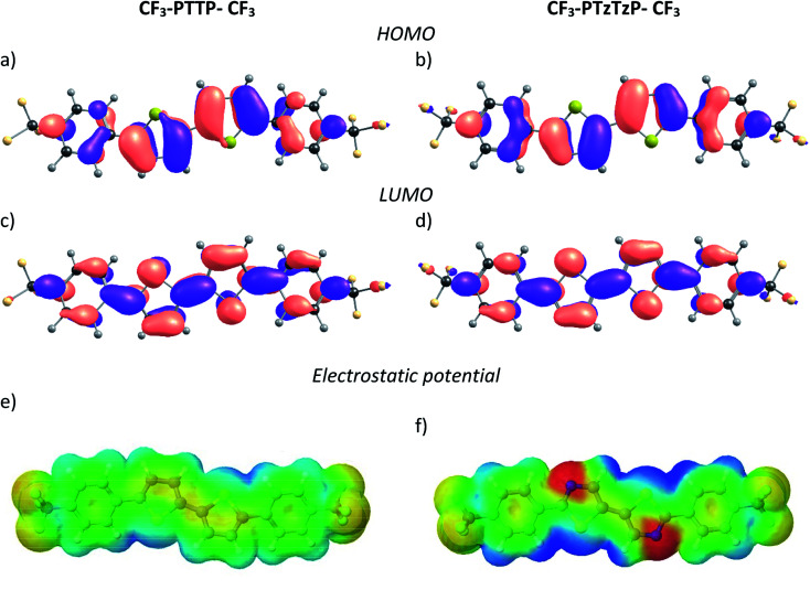
Properties of the organic semiconductors can be finely tuned via changes in their molecular structure. However, the relationship between the molecular structure, molecular packing, and (opto)electronic properties of the organic semiconductors to guide their smart design remains elusive. In this study, we address computationally and experimentally the impact of subtle modification of a thiophene-phenylene co-oligomer CF3-PTTP-CF3 on the molecular properties, crystal structure, charge transport, and optoelectronic properties. This modification consists in the substitution of two C-H atom pairs by N atoms in the thiophene units and hence converting them to thiazole units. A dramatic effect of the N-substitution on the crystal structure-the crossover from the herringbone packing motif to π-stacking-is attributed to significant changes in the molecular electrostatic potential. The changes in the molecular and crystal structure resulting from the N-substitution clearly reveal themselves in the Raman spectra. The increase of the calculated electron mobility in the corresponding crystals as a result of the N-substitution is rationalized in terms of the changes in the molecular and crystal structure. The charge transport, electroluminescence, and photoelectric properties are compared in thin-film organic field-effect transistors based on CF3-PTTP-CF3 and its N-substituted counterpart. An intriguing similarity between the effects of N-substitution in the thiophene rings and fluorination of the thiophene-phenylene oligomer is revealed, which is probably associated with a more general effect of electronegative substitution. The obtained results are anticipated to facilitate the rational design of organic semiconductors.
This journal is © The Royal Society of Chemistry.
Conflict of interest statement
There are no conflicts to declare.
Figures


Similar articles
-
Tuning of Molecular Electrostatic Potential Enables Efficient Charge Transport in Crystalline Azaacenes: A Computational Study.Int J Mol Sci. 2020 Aug 6;21(16):5654. doi: 10.3390/ijms21165654. Int J Mol Sci. 2020. PMID: 32781772 Free PMC article.
-
Fluorinated Thiophene-Phenylene Co-Oligomers for Optoelectronic Devices.ACS Appl Mater Interfaces. 2020 Feb 26;12(8):9507-9519. doi: 10.1021/acsami.9b20295. Epub 2020 Feb 14. ACS Appl Mater Interfaces. 2020. PMID: 32009377
-
Impact of terminal substituents on the electronic, vibrational and optical properties of thiophene-phenylene co-oligomers.Phys Chem Chem Phys. 2019 Jun 5;21(22):11578-11588. doi: 10.1039/c9cp00910h. Phys Chem Chem Phys. 2019. PMID: 30968108
-
Bithiazole: An Intriguing Electron-Deficient Building for Plastic Electronic Applications.Macromol Rapid Commun. 2017 May;38(10). doi: 10.1002/marc.201600610. Epub 2017 Mar 2. Macromol Rapid Commun. 2017. PMID: 28251727 Review.
-
Thiophene-Based Organic Semiconductors.Top Curr Chem (Cham). 2017 Oct 24;375(6):84. doi: 10.1007/s41061-017-0174-z. Top Curr Chem (Cham). 2017. PMID: 29063993 Review.
Cited by
-
High-Mobility Naphthalene Diimide Derivatives Revealed by Raman-Based In Silico Screening.Int J Mol Sci. 2022 Nov 1;23(21):13305. doi: 10.3390/ijms232113305. Int J Mol Sci. 2022. PMID: 36362092 Free PMC article.
-
Tuning of Molecular Electrostatic Potential Enables Efficient Charge Transport in Crystalline Azaacenes: A Computational Study.Int J Mol Sci. 2020 Aug 6;21(16):5654. doi: 10.3390/ijms21165654. Int J Mol Sci. 2020. PMID: 32781772 Free PMC article.
-
Dual Optoelectronic Organic Field-Effect Device: Combination of Electroluminescence and Photosensitivity.Molecules. 2024 May 28;29(11):2533. doi: 10.3390/molecules29112533. Molecules. 2024. PMID: 38893409 Free PMC article.
References
LinkOut - more resources
Full Text Sources
Research Materials
Miscellaneous