. 2022 May 6;13(1):2482.
doi: 10.1038/s41467-022-29958-2.

Mobility enhancement in heavily doped semiconductors via electron cloaking

Affiliations

Mobility enhancement in heavily doped semiconductors via electron cloaking

Jiawei Zhou et al. Nat Commun. .

Abstract

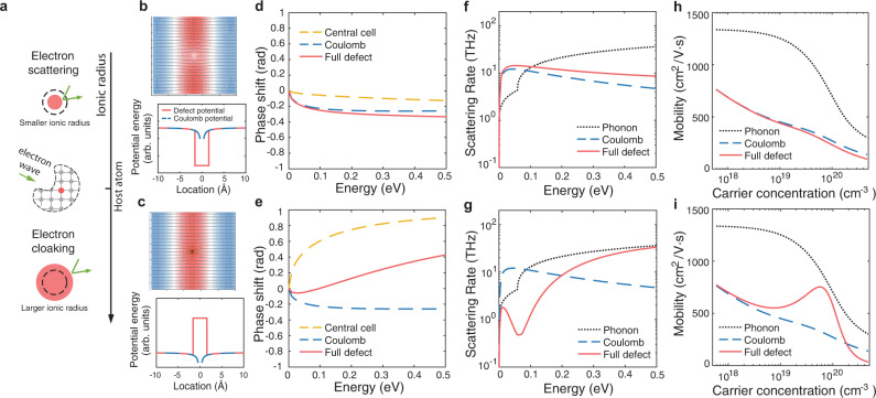
Doping is central for solid-state devices from transistors to thermoelectric energy converters. The interaction between electrons and dopants plays a pivotal role in carrier transport. Conventional theory suggests that the Coulomb field of the ionized dopants limits the charge mobility at high carrier densities, and that either the atomic details of the dopants are unimportant or the mobility can only be further degraded, while experimental results often show that dopant choice affects mobility. In practice, the selection of dopants is still mostly a trial-and-error process. Here we demonstrate, via first-principles simulation and comparison with experiments, that a large short-range perturbation created by selected dopants can in fact counteract the long-range Coulomb field, leading to electron transport that is nearly immune to the presence of dopants. Such "cloaking" of dopants leads to enhanced mobilities at high carrier concentrations close to the intrinsic electron-phonon scattering limit. We show that the ionic radius can be used to guide dopant selection in order to achieve such an electron-cloaking effect. Our finding provides guidance to the selection of dopants for solid-state conductors to achieve high mobility for electronic, photonic, and energy conversion applications.


Conflict of interest statement

The authors declare no competing interests.

Figures

Fig. 1
Fig. 1. Impact of charged defects on electron transport.
a Illustration of a propagating electron wave scattered by the perturbed electronic potential of an n-type dopant. The defect potential contains two parts, a long-range part due to the attractive Coulomb field, and a short-range part that depends on the bonding environment of the defect (the central cell potential). The ionic radius can be used as a good indicator for the sign of the central cell potential. Depending on the ionic radius of the dopant atom, one of two general scenarios can play out. If the dopant atom has a smaller ionic radius than the host atom, the perturbation tends to create an additional attractive force for electrons (electron-scattering scenario); if the dopant atom has a larger ionic radius, it tends to create a repulsive force which then opposes the long-range Coulomb potential (electron-cloaking scenario). b, c Defect potentials and scattered electron wavefunctions corresponding to two different scenarios (b: electron scattering, c: electron cloaking). The central cell potential is represented by a simplified rectangular profile. The streamlines show the probability flux and the colors indicate the real part of the wavefunctions. In the case of electron cloaking (c), unperturbed streamlines are recovered away from the defect (located at the center). The domain size is 158.8 Å × 158.8 Å and the electron energy is 0.1 eV. d, e Phase shifts of scattered wavefunctions with angular momentum quantum number of l = 1 for two scenarios (d: electron scattering, e: electron cloaking). f, g Modeled intrinsic electron scattering rates due to electron–phonon interactions, in comparison to those considering electron-defect scatterings (f: electron scattering, g: electron cloaking). The calculation assumes a parabolic band to illustrate the general impact of defect scatterings and uses partial wave analysis to calculate the scattering rates due to defects (see details in Methods). h, i Electron mobility with respect to the carrier concentration (h: electron scattering, i: electron cloaking). While mobility at high carrier concentrations is traditionally believed to be limited by Coulomb scattering, a strong opposing central cell potential can be harnessed to break this limit, leading to high mobility limited only by the intrinsic electron–phonon interactions, as shown in (i).
Fig. 2
Fig. 2. Electron-defect interaction.
a Ratio between characteristic electron scattering rates due to central cell scattering and those due to Coulomb scattering, η=γcent/γCoul, shown as a color map (with red indicating high η, blue indicating low η, and white indicating unity, as shown in the scale on the right), with respect to the dielectric constant and carrier concentration. The characteristic electron scattering rate γ is defined based on the mobility μ as γ=e/(m*μ). Studied materials in this work are also labeled in the plot. Both PbTe and SrTiO3 have large dielectric constants and the arrows indicate their actual locations lie outside the given dielectric constant range. Regions with η1 represent cases in which the central cell potential has a comparable impact on charge transport to that of the Coulomb potential, and thus could be harnessed to counteract the Coulomb scatterings. The magnitude of the central cell potential is taken to be 6 eV (with a width of 6 Bohr radius) in this simulation. b, c Contour plots of the electron-defect interaction matrix ψkV^ψk for (b) Si-doped GaAs and (c) Bi-doped PbTe, respectively, where (k) is taken to be at the conduction band edge state (at the Γ point for GaAs and at the L point for PbTe). Significant electron-defect interaction is seen for PbTe. The unit of the coordinates is Å and the center is at the defect location. d, e Computed electron mobility as a function of the carrier density for (d) n-type GaAs with two different dopants (Ga:Si, As:Te) and (e) n-type PbTe with two different dopants (Pb:Bi, Te:I) in comparison to experimental results [experimental sources: As:Te and Ga:Si; Te:I; Pb:Bi]. For PbTe, Bi doping strongly reduces the mobility compared to I doping, whereas the dopant effects on GaAs are comparatively smaller.
Fig. 3
Fig. 3. Defect-mediated electrical and thermoelectric transport.
a Correlation between ionic radius difference and the short-range electron-defect interaction matrix in half-Heusler materials with different dopants. Inset: relative sizes of the related atoms illustrated based on their ionic radius, with the corresponding charges shown at the top of each column. The electron-defect interaction matrix is calculated for the band edge state. b, c Compiled experimental data for mobility dependence on the carrier concentration in representative half-Heusler materials with different dopants: b n-type ZrNiSn [experimental sources: ZrNiSn:V; ZrNiSn:Nb,; Zr0.75Hf0.25NiSn:Nb; ZrNiSn:Ta,], and c p-type NbFeSb [experimental sources: NbFeSb: Ti,; NbFeSb:Zr and NbFeSb:Hf). d, e Compiled highest mobility data from past studies with respect to the ionic radius difference between the dopant and host atoms for (d) n-type ZrNiSn and (e) p-type NbFeSb [experimental sources: ZrNiSn:V; ZrNiSn:Ta,; ZrNiSn:Nb,; NbFeSb:Ti,,,; NbFeSb:Hf,; NbFeSb:Zr,,]. The ionic radius differences are taken from (a). The shaded regions indicate the standard deviation of these extracted mobility data. f, g Comparisons between simulations and experimental results for the (f) electrical conductivity and (g) thermoelectric power factor of Ti-doped NbFeSb from 300 to 1000 K. Consideration of Coulomb scatterings alone underestimates the power factor, while the consideration of full defect scattering with a partial cloaking effect leads to better agreement with the experiment. h Comparison between simulations and experimental results for the optimal room-temperature thermoelectric power factor in p-type NbFeSb with respect to the ionic radius difference between dopant and host atoms. The trend of power factor with respect to the ionic radius agrees between the experiments and the simulations.

References

    1. Sze, S. M. Physics of Semiconductor Devices (John Wiley & Sons, 1981).
    1. Brooks, H. Theory of the electrical properties of germanium and silicon. in Advances in Electronics and Electron Physics vol. 7 (ed. Marton, L.) 85–182 (Academic Press, 1955).
    1. Herring C. Transport properties of a many-valley semiconductor. Bell Syst. Tech. J. 1955;34:237–290. doi: 10.1002/j.1538-7305.1955.tb01472.x. - DOI
    1. Chattopadhyay D, Queisser HJ. Electron scattering by ionized impurities in semiconductors. Rev. Mod. Phys. 1981;53:745–768. doi: 10.1103/RevModPhys.53.745. - DOI
    1. Fischetti MV. Effect of the electron-plasmon interaction on the electron mobility in silicon. Phys. Rev. B. 1991;44:5527–5534. doi: 10.1103/PhysRevB.44.5527. - DOI - PubMed