

A route towards the fabrication of large-scale and high-quality perovskite films for optoelectronic devices
- PMID: 35523822
- PMCID: PMC9076914
- DOI: 10.1038/s41598-022-10790-z
A route towards the fabrication of large-scale and high-quality perovskite films for optoelectronic devices
Abstract
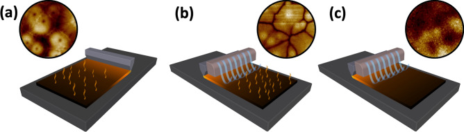
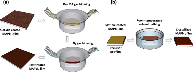
Halide perovskite materials have been extensively explored for their unique electrical, optical, magnetic, and catalytic properties. Most notably, solar cells based on perovskite thin films have improved their power conversion efficiency from 3.8% to over 25% during the last 12 years. However, it is still a challenge to develop a perovskite-based ink, suitable for upscaling the fabrication process of high-quality perovskite films with extreme purity, good crystallinity, and complete coverage over the deposition area. This is particularly important if the perovskite films are to be used for the scaled production of optoelectronic devices. Therefore, to make halide perovskites commercially available for various applications, it is vital to develop a reliable and highly robust deposition method, which can then be transferred to industry. Herein, the development of perovskite precursor inks suitable for use at low-temperature and vacuum-free solution-based deposition processes is reported. These inks can be further tailored according to the requirements of the deposition method, i.e., we propose their use with the industrially viable deposition technique called "slot-die coating". Furthermore, a route for the preparation of low-cost and high-volume manufacturing of perovskite films on both rigid and flexible substrates is suggested in this paper. The presented approach is suitable for the fabrication of any functional layers of perovskites, that can be employed in various scaled applications, and it seeks the potential and the methodology for perovskite film deposition that is scalable to industrial standards.
© 2022. The Author(s).
Conflict of interest statement
The authors declare no competing interests.
Figures


References
-
- Silva SRP. EDITORIAL: Now is the time for energy materials research to save the planet. Energy Environ. Mater. 2021;4:497–499. doi: 10.1002/eem2.12233. - DOI
-
- Correa-Baena J-P, et al. The rapid evolution of highly efficient perovskite solar cells. Energy Environ. Sci. 2017;10:710–727. doi: 10.1039/C6EE03397K. - DOI
-
- Dubey A, et al. A strategic review on processing routes towards highly efficient perovskite solar cells. J. Mater. Chem. A. 2018;6:2406–2431. doi: 10.1039/C7TA08277K. - DOI
-
- Green MA, Ho-Baillie A, Snaith HJ. The emergence of perovskite solar cells. Nat. Photon. 2014;8:506–514. doi: 10.1038/nphoton.2014.134. - DOI
LinkOut - more resources
Full Text Sources
