Synthesis, oxide formation, properties and thin film transistor properties of yttrium and aluminium oxide thin films employing a molecular-based precursor route
- PMID: 35527957
- PMCID: PMC9072413
- DOI: 10.1039/c9ra05348d
Synthesis, oxide formation, properties and thin film transistor properties of yttrium and aluminium oxide thin films employing a molecular-based precursor route
Abstract
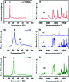
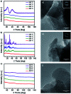
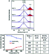
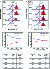
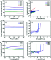
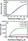
Combustion synthesis of dielectric yttrium oxide and aluminium oxide thin films is possible by introducing a molecular single-source precursor approach employing a newly designed nitro functionalized malonato complex of yttrium (Y-DEM-NO21) as well as defined urea nitrate coordination compounds of yttrium (Y-UN 2) and aluminium (Al-UN 3). All new precursor compounds were extensively characterized by spectroscopic techniques (NMR/IR) as well as by single-crystal structure analysis for both urea nitrate coordination compounds. The thermal decomposition of the precursors 1-3 was studied by means of differential scanning calorimetry (DSC) and thermogravimetry coupled with mass spectrometry and infrared spectroscopy (TG-MS/IR). As a result, a controlled thermal conversion of the precursors into dielectric thin films could be achieved. These oxidic thin films integrated within capacitor devices are exhibiting excellent dielectric behaviour in the temperature range between 250 and 350 °C, with areal capacity values up to 250 nF cm-2, leakage current densities below 1.0 × 10⁻⁹ A cm-2 (at 1 MV cm-1) and breakdown voltages above 2 MV cm-1. Thereby the increase in performance at higher temperatures can be attributed to the gradual conversion of the intermediate hydroxy species into the respective metal oxide which is confirmed by X-ray photoelectron spectroscopy (XPS). Finally, a solution-processed Y x O y based TFT was fabricated employing the precursor Y-DEM-NO21. The device exhibits decent TFT characteristics with a saturation mobility (μ sat) of 2.1 cm2 V-1 s-1, a threshold voltage (V th) of 6.9 V and an on/off current ratio (I on/off) of 7.6 × 10⁵.
This journal is © The Royal Society of Chemistry.
Conflict of interest statement
The authors declare no conflict of interests.
Figures





Similar articles
-
Aqueous Solution Processing of Combustible Precursor Compounds into Amorphous Indium Gallium Zinc Oxide (IGZO) Semiconductors for Thin Film Transistor Applications.Chem Asian J. 2018 Dec 18;13(24):3912-3919. doi: 10.1002/asia.201801371. Epub 2018 Nov 13. Chem Asian J. 2018. PMID: 30426698
-
Facile and environmentally friendly solution-processed aluminum oxide dielectric for low-temperature, high-performance oxide thin-film transistors.ACS Appl Mater Interfaces. 2015 Mar 18;7(10):5803-10. doi: 10.1021/am508775c. Epub 2015 Mar 3. ACS Appl Mater Interfaces. 2015. PMID: 25679286
-
Exploratory combustion synthesis: amorphous indium yttrium oxide for thin-film transistors.J Am Chem Soc. 2012 Jun 13;134(23):9593-6. doi: 10.1021/ja303589v. Epub 2012 Jun 1. J Am Chem Soc. 2012. PMID: 22625409
-
Atomic layer deposition of dielectric Y2O3 thin films from a homoleptic yttrium formamidinate precursor and water.RSC Adv. 2021 Jan 12;11(5):2565-2574. doi: 10.1039/d0ra09876k. eCollection 2021 Jan 11. RSC Adv. 2021. PMID: 35424225 Free PMC article.
-
Boron-doped peroxo-zirconium oxide dielectric for high-performance, low-temperature, solution-processed indium oxide thin-film transistor.ACS Appl Mater Interfaces. 2013 Aug 28;5(16):8067-75. doi: 10.1021/am402153g. Epub 2013 Aug 8. ACS Appl Mater Interfaces. 2013. PMID: 23883390
Cited by
-
Application of Solution-Processed High-Entropy Metal Oxide Dielectric Layers with High Dielectric Constant and Wide Bandgap in Thin-Film Transistors.Micromachines (Basel). 2024 Nov 30;15(12):1465. doi: 10.3390/mi15121465. Micromachines (Basel). 2024. PMID: 39770218 Free PMC article.
-
Mo(vi) complexes of amide-imine conjugates for tuning the selectivity of fluorescence recognition of Y(iii) vs. Pb(ii).RSC Adv. 2022 Nov 21;12(51):33293-33303. doi: 10.1039/d2ra06035c. eCollection 2022 Nov 15. RSC Adv. 2022. PMID: 36425161 Free PMC article.
References
-
- Facchetti A. and Marks T. J., Transparent Electronics: From Synthesis to Applications, 2010
-
- Park S. Kim C.-H. Lee W.-J. Sung S. Yoon M.-H. Mater. Sci. Eng., R. 2017;114:1–22. doi: 10.1016/j.mser.2017.01.003. - DOI
-
- Robertson J. Wallace R. M. Mater. Sci. Eng., R. 2015;88:1–41. doi: 10.1016/j.mser.2014.11.001. - DOI
-
- Xu W. Wang H. Ye L. Xu J. J. Mater. Chem. C. 2014;2:5389–5396. doi: 10.1039/C4TC00334A. - DOI
-
- Frunză R. C. Kmet B. Jankovec M. Topič M. Malič B. Mater. Res. Bull. 2014;50:323–328. doi: 10.1016/j.materresbull.2013.11.025. - DOI
LinkOut - more resources
Full Text Sources
Research Materials
Miscellaneous

