Review
. 2019 Aug 28;9(46):26961-26980.
doi: 10.1039/c9ra04404c. eCollection 2019 Aug 23.

Recent progress of solution-processed Cu nanowires transparent electrodes and their applications

Affiliations
Review

Recent progress of solution-processed Cu nanowires transparent electrodes and their applications

Su Ding et al. RSC Adv. .

Abstract

Research on next-generation transparent electrode (TE) materials to replace expensive and fragile indium tin oxide (ITO) is crucial for future electronics. Copper nanowires (Cu NWs) are considered as one of the most promising alternatives due to their excellent electrical properties and low-cost processing. This review summarizes the recent progress on the synthesis methods of long Cu NWs, and the fabrication techniques and protection measures for Cu NW TEs. Applications of Cu NW TEs in electronics, such as solar cells, touch screens, and light emitting diodes (LEDs), are discussed.


Conflict of interest statement

There are no conflicts to declare.

Figures

Fig. 1
Fig. 1. Schematic of hydrothermal synthesis of 1D Cu NWs.
Fig. 2
Fig. 2. Synthesis of Cu NWs using EDA as a surfactant. (a) A photograph of a Cu NW solution. (b) An scanning electron microscopy (SEM) image of Cu NWs. (c) The growth model of the Cu NWs.
Fig. 3
Fig. 3. Fabrication of Cu NW TEs and the characterization of their properties. (a) A bent Cu NW film completing an electrical circuit with a battery pack and an LED. (b) An SEM image showing a uniformly dispersed network of Cu NWs that was 85% transparent with a Rsh of 30 ohm sq−1. (c) A plot of T versus Rsh for Cu NW TEs. (d) A plot of Rshversus number of bends for Cu NW TEs.
Fig. 4
Fig. 4. (a) SEM images of the Cu NW TEs on glass substrates with a transmittance at 87%, (b) AFM image of Cu NW after annealing at 200 °C for 1 h, where the welding point has been formed, and schematic of the nanowelding between two NWs before and after annealing. (c) and (d) Transmittance verse Rsh for the Cu NW TEs which were annealed at 150 °C and 200 °C, respectively, and exposed in air for 30 days.
Fig. 5
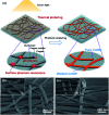
Fig. 5. (a) SEM image of Cu NW films. (b) SEM image of lactic acid treated Cu NW TEs. (c) Schematic illustration of the lactic treatment process.
Fig. 6
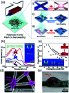
Fig. 6. Fabrication of Cu NW TEs by laser plasmonic nanowelding method. (a) Schematic illustrations of the plasmonic laser nanowelding process; (b) optical and SEM images (insets) of as-prepared, laser-nanowelded, and bulk-heated Cu NW films; (c) schematic illustration and optical photographs of the “nanorecycling” process.
Fig. 7
Fig. 7. (a) Schematic representation of the HIPL treatment of a Cu NW TE; SEM images of a Cu NW network (b) before and (c) after the HIPL treatment.
Fig. 8
Fig. 8. (a) Schematic illustration of the Cu NW plasmonic-tuned flash welding (PFW) process. (b) Spectral and polarization-dependent simulations of local light absorption for the Cu NW junction from 400 to 800 nm wavelength. The inset shows the field enhancement response under the visible light (wavelength of 600 nm) for light polarized perpendicular/parallel to the first NW. (c) Local heat generation as a function of Cu NW overlap length, which shows the self-limiting nature of the PFW process. The insets show field distribution simulations as a function of Cu NW overlap length. (d) A plane-view SEM image of PFW-treated Cu NWs. (e) A plane-view transmission electron microscope (TEM) image of fused Cu NW junction.
Fig. 9
Fig. 9. SEM images of Cu NWs (a) before and (b) after the coating of Ni to a concentration of 54%. The insets show the cross-sections of the Cu NW and CuNi NW. (c) Plot of T verse Rsh for films of Cu NWs, CuNi NWs, and ITO on glass. (d) Plot of Rshverse time for films of Ag NWs, Cu NWs, and CuNi NWs stored at 85 °C.
Fig. 10
Fig. 10. (a) Schematic illustration for the synthesis of the Cu NW–graphene core–shell nanostructure by the LT-PECVD process. (b) TEM image of the Cu NW–graphene core–shell nanostructure. (c) Energy disperse spectroscopy (EDS) mapping analysis of a Cu NW–graphene core–shell nanostructure. (d) Rsh changes for Cu NW and Cu NW–graphene TEs during a stability test in air at room temperature for 30 days.
Fig. 11
Fig. 11. AFM topographic images of (a) Cu NW TEs and (b) Cu NW/polymer composite TEs. (c) Change in Rsh of Cu NW and Cu NW/PMMA composite TEs stored under ambient conditions for 30 days. (d) Changes in the current of Cu NW and Cu NW/polymer composite TEs over time, upon treatment with aqueous Na2S solution.
Fig. 12
Fig. 12. Resistance change of the simply coated and laser-nanowelded Cu NW electrodes at different strains. Inset shows the corresponding optical images under various strains.
Fig. 13
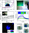
Fig. 13. Applications of Cu NW TEs. (a) Characteristic IV curves of solar cells with ITO or a Cu NW film as the transparent electrode. The inset shows the photograph of a flexible solar cell. (b) Demonstration of a touch-screen panel fabricated with a laser-nanowelded Cu NW TE. (c) Application of Cu NW/PU conductors in a strain sensor recording the relative resistance response of Cu NW/PU conductors to the bending and releasing of a finger. (d) Temperature profiles as a function of applied voltage of 3, 5, and 7 V on the Cu NW/PU heater. (e) Optical image of the blue light electroluminescence of an InGaN-based LED with Cu NW TEs. (f) An as-prepared mixed transparent electrode composed of a pure Cu NW film (left) and RGO/Cu NW film (right). The initial (coloured) state (right-top) and bleached state (right-bottom) of PB deposited on the mixed electrode.

Similar articles

Cited by

References

    1. Kim Y. H. Lee J. Hofmann S. Gather M. C. Müller-Meskamp L. Leo K. Adv. Funct. Mater. 2013;23:3763–3769. doi: 10.1002/adfm.201203449. - DOI
    1. Li N. Oida S. Tulevski G. S. Han S. J. Hannon J. B. Sadana D. K. Chen T. C. Nat. Commun. 2013;4:2294. doi: 10.1038/ncomms3294. - DOI - PubMed
    1. Tae Lim J. Lee H. Cho H. Kwon B. H. Sung Cho N. Kuk Lee B. Park J. Kim J. Han J. H. Yang J. H. Yu B. G. Hwang C. S. Chu Lim S. Lee J. I. Sci. Rep. 2015;5:17748. doi: 10.1038/srep17748. - DOI - PMC - PubMed
    1. Naghdi S. Rhee K. Hui D. Park S. Coatings. 2018;8:278. doi: 10.3390/coatings8080278. - DOI
    1. Huang Y. Huang Z. Zhong Z. Yang X. Hong Q. Wang H. Huang S. Gao N. Chen X. Cai D. Kang J. Sci. Rep. 2018;8:13721. doi: 10.1038/s41598-018-31903-7. - DOI - PMC - PubMed