Review
. 2019 Aug 16;9(44):25439-25461.
doi: 10.1039/c9ra03769a. eCollection 2019 Aug 13.

Retracted Article: Physics of excitons and their transport in two dimensional transition metal dichalcogenide semiconductors

Affiliations
Review

Retracted Article: Physics of excitons and their transport in two dimensional transition metal dichalcogenide semiconductors

Bhaskar Kaviraj et al. RSC Adv. .

Abstract

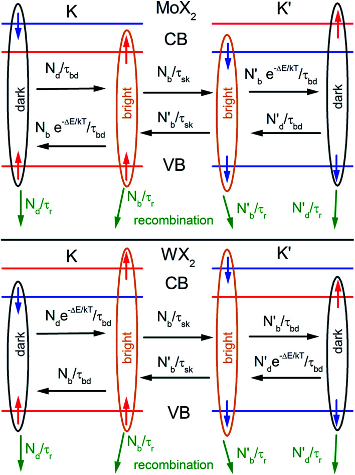
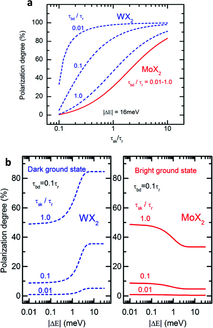
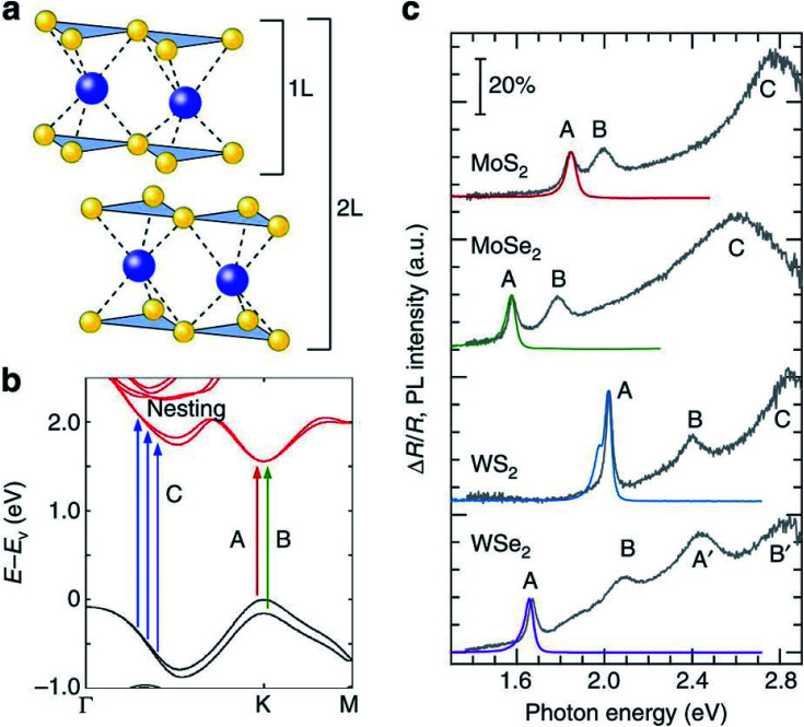
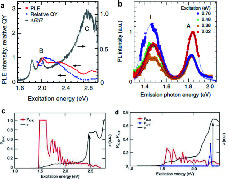
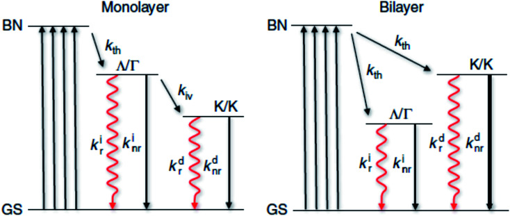
Two-dimensional (2D) group-VI transition metal dichalcogenide (TMD) semiconductors, such as MoS2, MoSe2, WS2 and others manifest strong light matter coupling and exhibit direct band gaps which lie in the visible and infrared spectral regimes. These properties make them potentially interesting candidates for applications in optics and optoelectronics. The excitons found in these materials are tightly bound and dominate the optical response, even at room temperatures. Large binding energies and unique exciton fine structure make these materials an ideal platform to study exciton behaviors in two-dimensional systems. This review article mainly focuses on studies of mechanisms that control dynamics of excitons in 2D systems - an area where there remains a lack of consensus in spite of extensive research. Firstly, we focus on the kinetics of dark and bright excitons based on a rate equation model and discuss on the role of previous 'unsuspected' dark excitons in controlling valley polarization. Intrinsically, dark and bright exciton energy splitting plays a key role in modulating the dynamics. In the second part, we review the excitation energy-dependent possible characteristic relaxation pathways of photoexcited carriers in monolayer and bilayer systems. In the third part, we review the extrinsic factors, in particular the defects that are so prevalent in single layer TMDs, affecting exciton dynamics, transport and non-radiative recombination such as exciton-exciton annihilation. Lastly, the optical response due to pump-induced changes in TMD monolayers have been reviewed using femtosecond pump-probe spectroscopy which facilitates the analysis of underlying physical process just after the excitation.


Conflict of interest statement

There are no conflicts to declare.

Figures

Fig. 1
Fig. 1. Schematic showing the band structure and spin configuration of the bright and dark A-excitons in MoX2 and WX2 materials. The possible inter and intra valley scattering and recombination paths included in the rate equations (see text) are indicated schematically. The influence of B-excitons can safely be neglected due to the large spin–orbit splitting in the valence band. (Adapted with permission from ref. 64 Copyright 2017 IOP Publishing).
Fig. 2
Fig. 2. (a) Degree of circular polarization in PL as a function of the inter-valley scattering time calculated using the rate equations for WX2 (broken lines) and MoX2 (solid lines) for three different values of the bright–dark exciton scattering time τbd. (b) Dependence of PL circular polarization degree as function of absolute value of bright–dark exciton spin splitting calculated according to rate eqn (3) (WX2) and eqn (4) (MoX2) for different values of inter-valley scattering time. (Adapted with permission from ref. 64 Copyright 2017 IOP Publishing).
Fig. 3
Fig. 3. Properties of monolayer MX2. (a) Lattice structures of monolayer and bilayer MX2. (b) The band structure of monolayer MoS2 with the label of C calculated by the DFT. The arrows indicate the transition in A, B and the band nesting (C). (c) PL spectra (red, green, blue and purple curves) from excitation at the C (A′ for WSe2) peak and differential reflectance spectra (grey curves) of monolayer MX2 flakes on quartz substrates. The scale bar indicates 20% absorption based on the differential reflectance spectra. The PL intensity is normalized by the A exciton peak of the differential reflectance spectra for each material and the spectra are displaced along the vertical axis for clarity. (Adapted with permission from ref. 92 Copyright 2014 Macmillan Publishers).
Fig. 4
Fig. 4. (a) PLE spectra and relative QY of emission for band gap emission for monolayer MoS2 flakes. Differential reflectance spectra are also shown for comparison. The PLE spectra are based on the integrated intensity of the A peak in the PL spectra at each excitation energy. The PLE spectrum is normalized by the B exciton peak of the material. (b) PL spectra of bilayer MoS2 flake collected with excitation energy of 2.02, 2.38, 2.48, 2.76 eV. (c, d) The fraction of electron–hole pairs that end the relaxation at the K point (PK_K, red curve) and the optical conductivity (σ, black curve) for monolayer (c) and bilayer MoS2 (d). For (d), the fraction of electron–hole pairs relaxing to Λ valley and Γ hill (PΛ_Γ) is also shown (blue plot). The black arrows indicate the position of the first peak due to band nesting. (Adapted with permission from ref. 92 Copyright 2014 Macmillan Publishers).
Fig. 5
Fig. 5. Excitation and relaxation pathways for photocarriers. Energy diagram representing photocarrier relaxation channels in monolayer and bilayer MX2 where the initial excitation is from the ground state (GS) to the band nesting (BN) energy. Nonradiative transition is indicated with a black solid arrow. A rate constant k is associated with each transition. The subscripts indicate the types of transition: intravalley thermalization (kth), intervalley scattering (kiv), radiative (kr) and nonradiative (knr). The superscripts (i) and (d) indicate indirect and direct transitions, respectively.
Fig. 6
Fig. 6. (a) TA dynamics of a suspended exfoliated 1L-MoS2 flake. Red line is a fit using a triexponential function convoluted with an experimental response function. Pump fluence is 0.6 μJ cm−2. (b) TA dynamics of exfoliated 1L-WS2 on SiO2 substrate and CVD 1L-WS2 on sapphire. Red lines are fits using a biexponential function convoluted with an experimental response function. Pump fluence is 1 μJ cm−2. (Adapted with permission from ref. 104 Copyright 2017 ACS Publications).
Fig. 7
Fig. 7. (a) Schematic description of the exciton diffusion measurements. Spatial profiles of excitons in an exfoliated 1L-WS2 (b) and a CVD 1L-WS2 (c) at different pump–probe delay times. (d) Diffusion constants are obtained from the linear fitting of the variance of Gaussian profiles using eqn (12). Red lines are the linear fits. (e) Extracted decay constants and exciton diffusion constants are plotted as a function of number of layers. (f) Thickness-dependent exciton dynamics are modeled by eqn (10). (Adapted with permission from ref. 104 Copyright 2017 ACS Publications).
Fig. 8
Fig. 8. Quantitative analysis of the time-dependent line shape of the A exciton resonance in WS2 monolayer. (a) Representative reflectance contrast spectrum fitted with a Lorentzian line shape (red line) and linear offset (green line). (b) Relative changes of the line width Δw/w0, area ΔA/A0, and resonance energy ΔE/E0 of the peak are presented as a function of time delay for a pump fluence of 101 μJ cm−2. The data are normalized to the corresponding values at negative delay times: w0 = 47 meV, A0 = 1 arb unit, and E0 = 1.996 eV. (inset) The relative change of the line width and area for short delay times. Lower panel: The relative change of the reflectance contrast RC at a probe energy of 1.997 eV, averaged over a narrow spectral range of 13 meV, is shown for comparison. (Adapted with permission from ref. 138 Copyright 2017 ACS Publications).
Fig. 9
Fig. 9. Band profiles of p–n junctions in bulk and atomically thin materials. (a) In atomically thin monolayer, there is a sharp discontinuity at the interface of a p- and n-type material (left panel) whereas band bending occurs inside the depletion region in p–n junctions of bulk conventional semiconductors. (b) Band profiles under equilibrium (no external bias), forward and reverse bias in bulk p–n junctions. (c and d) Schematic diagrams of interlayer recombination (c) in a monolayer–monolayer p–n junction and of (d) exciton dissociation process. Adapted with permission from ref. 157 Copyright 2018 Royal Society of Chemistry.
Fig. 10
Fig. 10. Electroluminescent devices (a) electroluminescence (EL) emission spectra of monolayer WSe2 electrostatic p–n junctions with split gate electrodes recorded for constant currents of 50, 100 and 200 nA. Green curve demonstrates no light emission obtained under unipolar (n-type) conduction. (Adapted with permission from ref. 34 Copyright 2014 Nature Publishing Group). (b) Comparison between EL and PL spectra of graphene/hBN/TMD/graphene vdW heterostructure. Inset shows the device structure. The light brown TMD layer is sandwiched by two hBN layers. The outermost electrodes are composed of graphene. (Adapted with permission from ref. 161 Copyright 2015 Nature Publishing Group). (c) Graphene/hBN/TMD device showing a narrow emission line from a localized exciton state (top). Photon correlation measurements of the EL showing photon antibunching (bottom). Inset shows the corresponding device structure. (Adapted with permission from ref. 178 Copyright 2016 ACS Publications).
Fig. 11
Fig. 11. Valley Hall effect based optoelectronics. (a) Schematics of valley-dependent optical selection rules and the electrons at the K and K′ valleys that possess opposite Berry curvatures . The orange arrows represent clockwise hopping motions of the K and K′ electrons. (b) Experimental demonstration of photoinduced valley Hall effect with the image of a Hall bar device. (c) Two-point (dashed line, Vx = 0.5 V) and four-point (solid line) conductivities of the device as a function of back gate voltage Vg. (Inset) Source–drain bias (Vx) dependence of the current along the longitudinal channel (Ix) at different back gate voltages Vg. (d) In monolayer MoS2, the sign of photovoltage produced in a Hall bar depends on the helicity of light, whereas the effect is absent in a bilayer or for linear polarization (Fig. 10(a)–(d): adapted with permission from ref. 193 Copyright 2014 American Association for the Advancement of Science). (e) Valley polarization by spin injection. Monolayer WSe2 is contacted using a ferromagnetic electrode (permalloy). MoS2 is transferred on top of the MoS2 channel, forming a heterojunction diode. Under the application of a positive bias voltage to the permalloy electrode, holes are injected from the permalloy electrode and recombine in the junction with electrons injected from the MoS2 side, resulting in light emission. (f) Spin-polarized charge carrier injection from a ferromagnetic electrode into a vdW heterostructure light emitter leads to circularly polarized light emission that can be tuned by an external magnetic field. (Fig. 10(e) and (f): adapted with permission from ref. 178 Copyright 2016 ACS Publications).

Similar articles

Cited by

References

    1. Frindt R. Yoffe A. Proc. R. Soc. London, Ser. A. 1963;273:69. doi: 10.1098/rspa.1963.0075. - DOI
    1. Fortin E. Sears W. J. Phys. Chem. Solids. 1982;43:881. doi: 10.1016/0022-3697(82)90037-3. - DOI
    1. Novoselov K. S. Geim A. K. Morozov S. V. Jiang D. Zhang Y. Dubonos S. V. Grigorieva I. V. Firsov A. A. Science. 2004;306:666. doi: 10.1126/science.1102896. - DOI - PubMed
    1. Novoselov K. Jiang D. Schedin F. Booth T. Khotkevich V. Morozov S. Geim A. Proc. Natl. Acad. Sci. U. S. A. 2005;102:10451. doi: 10.1073/pnas.0502848102. - DOI - PMC - PubMed
    1. Mak K. F. Lee C. Hone J. Shan J. Heinz T. F. Phys. Rev. Lett. 2010;105:136805. doi: 10.1103/PhysRevLett.105.136805. - DOI - PubMed