

Oxide-assisted growth of scalable single-crystalline graphene with seamlessly stitched millimeter-sized domains on commercial copper foils
- PMID: 35539852
- PMCID: PMC9078575
- DOI: 10.1039/c8ra00770e
Oxide-assisted growth of scalable single-crystalline graphene with seamlessly stitched millimeter-sized domains on commercial copper foils
Abstract
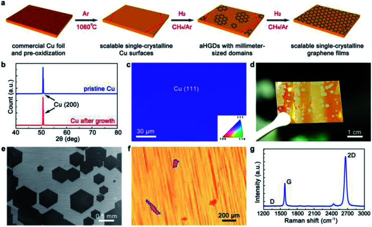
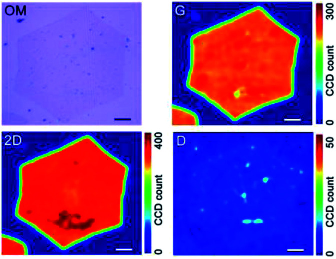
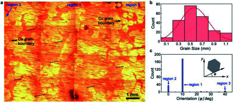
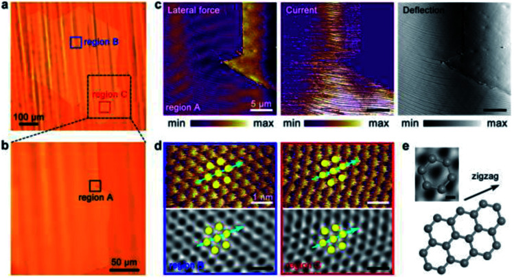
Chemical vapor deposition (CVD) is considered as an effective route to obtain large-area and high-quality polycrystalline graphene; however, there are still technological challenges associated with its application to achieve single crystals of graphene. Herein, we present the CVD growth of scalable single-crystalline graphene by seamless stitching millimeter-sized unidirectional aligned hexagonal domains using different types of commercial Cu foils without repeated substrate polishing and H2-annealing processes. Compared with that reported in previous studies, herein, the average size for the hexagonal graphene domains is enlarged by 1-2 orders of magnitude (from tens of micrometers to millimeter). The key factor for growth is the Cu surface monocrystallization achieved by a pre-introduced oxide layer and the sequential Ar annealing. The graphene domains exhibit an average growth rate of >20 μm min-1 and a misorientation possibility of <2%, and seamless stitching at the domain coalescence interfaces is confirmed by atomic force microscopy measurements.
This journal is © The Royal Society of Chemistry.
Conflict of interest statement
There are no conflicts to declare.
Figures
Similar articles
-
Surface Monocrystallization of Copper Foil for Fast Growth of Large Single-Crystal Graphene under Free Molecular Flow.Adv Mater. 2016 Oct;28(40):8968-8974. doi: 10.1002/adma.201603579. Epub 2016 Aug 26. Adv Mater. 2016. PMID: 27562642
-
Growth of Single-Layer and Multilayer Graphene on Cu/Ni Alloy Substrates.Acc Chem Res. 2020 Apr 21;53(4):800-811. doi: 10.1021/acs.accounts.9b00643. Epub 2020 Mar 24. Acc Chem Res. 2020. PMID: 32207601
-
Chemical vapor deposition of graphene single crystals.Acc Chem Res. 2014 Apr 15;47(4):1327-37. doi: 10.1021/ar4003043. Epub 2014 Feb 17. Acc Chem Res. 2014. PMID: 24527957
-
Roles of Oxygen and Hydrogen in Crystal Orientation Transition of Copper Foils for High-Quality Graphene Growth.Sci Rep. 2017 Apr 3;7:45358. doi: 10.1038/srep45358. Sci Rep. 2017. PMID: 28367988 Free PMC article.
-
Toward Epitaxial Growth of Misorientation-Free Graphene on Cu(111) Foils.ACS Nano. 2022 Jan 25;16(1):285-294. doi: 10.1021/acsnano.1c06285. Epub 2021 Dec 29. ACS Nano. 2022. PMID: 34965103
Cited by
-
Continuous orientated growth of scaled single-crystal 2D monolayer films.Nanoscale Adv. 2021 Oct 29;3(23):6545-6567. doi: 10.1039/d1na00545f. eCollection 2021 Nov 24. Nanoscale Adv. 2021. PMID: 36132651 Free PMC article. Review.
-
Adjusting the Morphology and Properties of SiC Nanowires by Catalyst Control.Materials (Basel). 2020 Nov 17;13(22):5179. doi: 10.3390/ma13225179. Materials (Basel). 2020. PMID: 33212809 Free PMC article.
-
Strain engineering of graphene on rigid substrates.Nanoscale Adv. 2022 Oct 12;4(23):5056-5061. doi: 10.1039/d2na00580h. eCollection 2022 Nov 22. Nanoscale Adv. 2022. PMID: 36504754 Free PMC article.
References
-
- Tapasztó L. Nemes-Incze P. Dobrik G. Jae Yoo K. Hwang C. Biró L. P. Appl. Phys. Lett. 2012;100:053114. doi: 10.1063/1.3681375. - DOI
LinkOut - more resources
Full Text Sources
Other Literature Sources
Research Materials
Miscellaneous