

Nanofluidic devices prepared by an atomic force microscopy-based single-scratch approach
- PMID: 35540223
- PMCID: PMC9075969
- DOI: 10.1039/c9ra06428a
Nanofluidic devices prepared by an atomic force microscopy-based single-scratch approach
Abstract
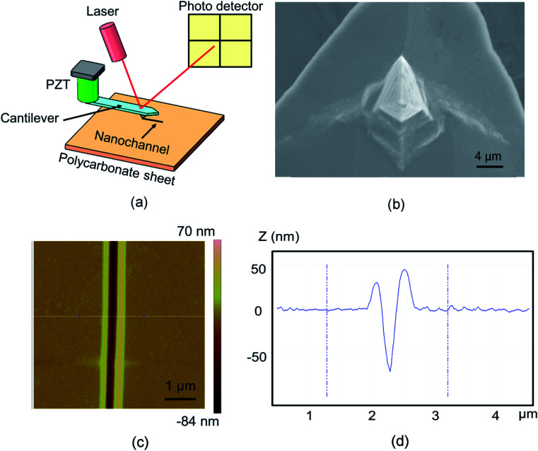
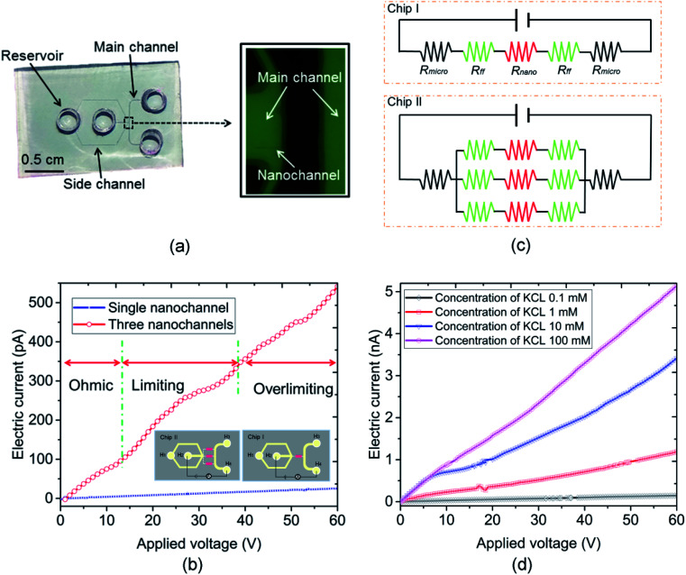
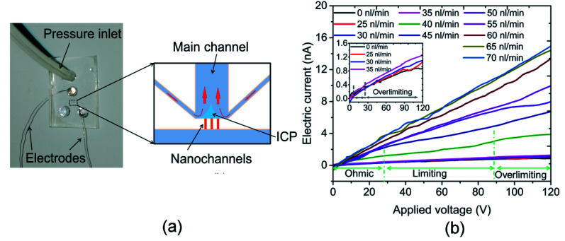
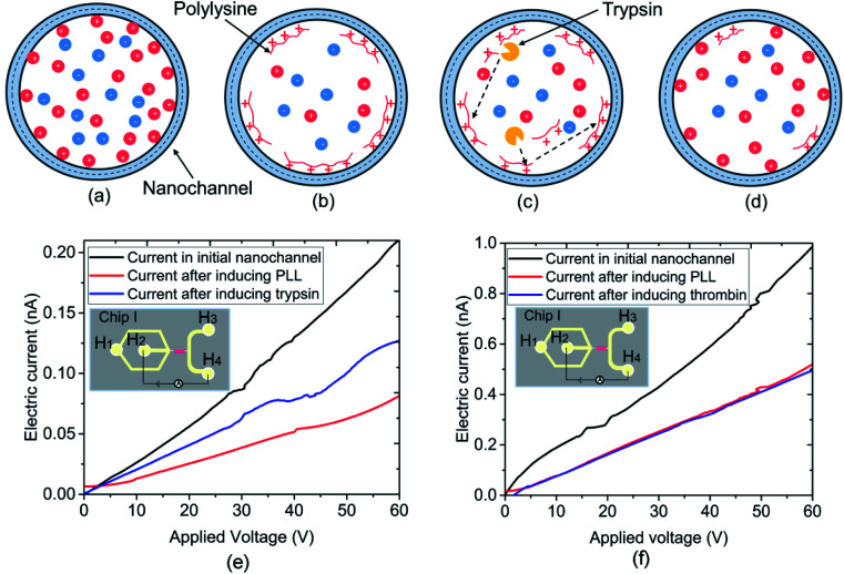
Nanofluidic chips with different numbers of nanochannels were fabricated based on a commercial AFM system using a single-scratch approach. The electrical characterization and enzymatic reactions at the nanoscale were demonstrated using the obtained chips. The effects of the number of nanochannels and the solution concentration on the measured electric current were investigated. The influence of the hydrodynamic convection generated from the induced inflow at the end of the nanochannel on the ion transport through the nanochannel was also studied. Moreover, the enzymatic reactions for trypsin towards poly-l-lysine (PLL) or thrombin were conducted with a nanofluidic chip to investigate the reaction specificity between trypsin and PLL. Results show that the electric current change during the experimental process could be used as a label-free indicator to detect the enzymatic activity.
This journal is © The Royal Society of Chemistry.
Conflict of interest statement
There are no conflicts to declare.
Figures
Similar articles
-
Fabrication of polydimethylsiloxane nanofluidic chips under AFM tip-based nanomilling process.Nanoscale Res Lett. 2019 Apr 17;14(1):136. doi: 10.1186/s11671-019-2962-6. Nanoscale Res Lett. 2019. PMID: 30997583 Free PMC article.
-
Label-Free Electrical Detection of Enzymatic Reactions in Nanochannels.ACS Nano. 2016 Aug 23;10(8):7476-84. doi: 10.1021/acsnano.6b02062. Epub 2016 Aug 5. ACS Nano. 2016. PMID: 27472431
-
A surface charge governed nanofluidic diode based on a single polydimethylsiloxane (PDMS) nanochannel.J Colloid Interface Sci. 2021 Aug 15;596:54-63. doi: 10.1016/j.jcis.2021.03.126. Epub 2021 Mar 24. J Colloid Interface Sci. 2021. PMID: 33831750
-
Fabrication of nanofluidic biochips with nanochannels for applications in DNA analysis.Small. 2012 Sep 24;8(18):2787-801. doi: 10.1002/smll.201200240. Epub 2012 Jul 9. Small. 2012. PMID: 22778064 Review.
-
Asymmetric ion transport through ion-channel-mimetic solid-state nanopores.Acc Chem Res. 2013 Dec 17;46(12):2834-46. doi: 10.1021/ar400024p. Epub 2013 May 28. Acc Chem Res. 2013. PMID: 23713693 Review.
References
-
- Fan Y. Deng C. Chung P. Tian W. Sheen H. Sens. Actuators, B. 2018;272:502–509. doi: 10.1016/j.snb.2018.05.141. - DOI
LinkOut - more resources
Full Text Sources
Miscellaneous