

Bridged oxide nanowire device fabrication using single step metal catalyst free thermal evaporation
- PMID: 35540462
- PMCID: PMC9078917
- DOI: 10.1039/c7ra11987a
Bridged oxide nanowire device fabrication using single step metal catalyst free thermal evaporation
Abstract
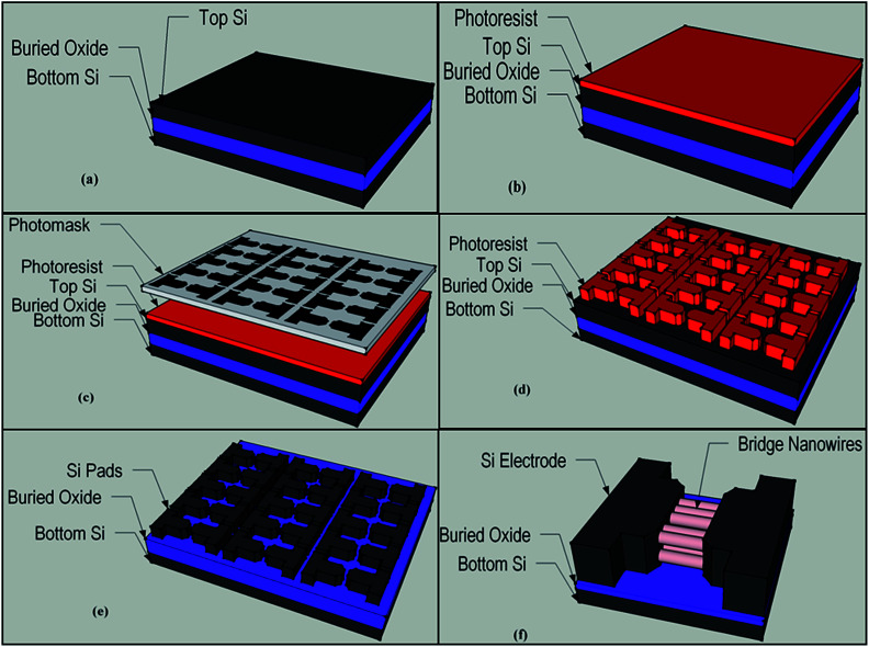
In this study, indium-tin-zinc-oxide (ITZO) and Zn doped In2O3 nanowires were directly grown as bridged nanowires between two heavily doped silicon (Si) electrodes on an SOI wafer using single step vapor-solid-solid (VSS) growth method. SEM analysis showed highly dense and self aligned nanowire formation between the Si electrodes. Electrical and UV response measurements were performed in ambient condition. Current-voltage characteristics of devices exhibited both linear and non-linear behavior. This was the first demonstration of bridged ITZO and Zn-doped In2O3 nanowires. Our results show that bridged nanowire growth technique can be a potential candidate for high performance electronic and optoelectronic devices.
This journal is © The Royal Society of Chemistry.
Conflict of interest statement
There are no conflicts to declare.
Figures


Similar articles
-
Self catalytic growth of indium oxide (In2O3) nanowires by resistive thermal evaporation.J Nanosci Nanotechnol. 2014 Jul;14(7):5485-90. doi: 10.1166/jnn.2014.8696. J Nanosci Nanotechnol. 2014. PMID: 24758054
-
In Situ Assembly of Ordered Hierarchical CuO Microhemisphere Nanowire Arrays for High-Performance Bifunctional Sensing Applications.Small Methods. 2021 Jun;5(6):e2100202. doi: 10.1002/smtd.202100202. Epub 2021 Apr 30. Small Methods. 2021. PMID: 34927905
-
Growth of epitaxial silicon nanowires on a Si substrate by a metal-catalyst-free process.Sci Rep. 2016 Jul 28;6:30608. doi: 10.1038/srep30608. Sci Rep. 2016. PMID: 27465800 Free PMC article.
-
The effect of doping on low temperature growth of high quality GaAs nanowires on polycrystalline films.Nanotechnology. 2016 Dec 9;27(49):495605. doi: 10.1088/0957-4484/27/49/495605. Epub 2016 Nov 11. Nanotechnology. 2016. PMID: 27834310 Free PMC article.
-
Controlled Synthesis and Enhanced Gas Sensing Performance of Zinc-Doped Indium Oxide Nanowires.Nanomaterials (Basel). 2023 Mar 25;13(7):1170. doi: 10.3390/nano13071170. Nanomaterials (Basel). 2023. PMID: 37049264 Free PMC article.
Cited by
-
Formation of sub-100-nm suspended nanowires with various materials using thermally adjusted electrospun nanofibers as templates.Microsyst Nanoeng. 2023 Feb 17;9:15. doi: 10.1038/s41378-022-00459-y. eCollection 2023. Microsyst Nanoeng. 2023. PMID: 36817329 Free PMC article.
References
-
- Oh J. Y. Islam M. S. Appl. Phys. Lett. 2014;104:022110. doi: 10.1063/1.4862328. - DOI