

Fully solution-induced high performance indium oxide thin film transistors with ZrO x high-k gate dielectrics
- PMID: 35540525
- PMCID: PMC9080338
- DOI: 10.1039/c8ra02108b
Fully solution-induced high performance indium oxide thin film transistors with ZrO x high-k gate dielectrics
Abstract
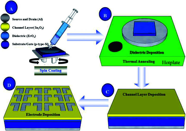
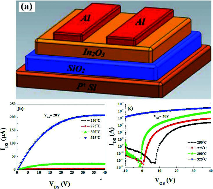
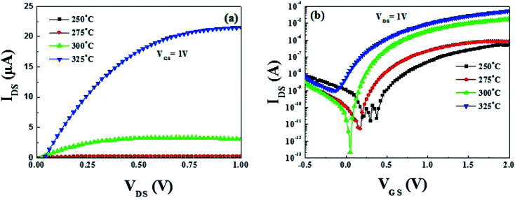
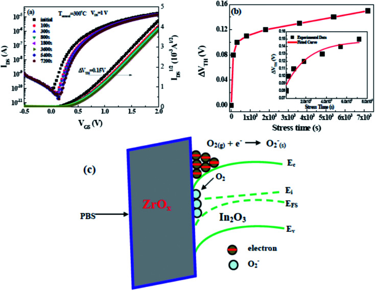
Solution based deposition has been recently considered as a viable option for low-cost flexible electronics. In this context, research efforts have been increasingly focused on the development of suitable solution-processed materials for oxide based transistors. In this work, we report a fully solution synthesis route, using 2-methoxyethanol as solvent, for the preparation of In2O3 thin films and ZrO x gate dielectrics, as well as the fabrication of In2O3-based TFTs. To verify the possible applications of ZrO x thin films as the gate dielectric in complementary metal oxide semiconductor (CMOS) electronics, fully solution-induced In2O3 TFTs based on ZrO2 dielectrics have been integrated and investigated. The devices, with an optimized annealing temperature of 300 °C, have demonstrated high electrical performance and operational stability at a low voltage of 2 V, including a high μ sat of 4.42 cm2 V-1 s-1, low threshold voltage of 0.31 V, threshold voltage shift of 0.15 V under positive bias stress for 7200 s, and large I on/I off of 7.5 × 10⁷, respectively. The as-fabricated In2O3/ZrO x TFTs enable fully solution-derived oxide TFTs for potential application in portable and low-power consumption electronics.
This journal is © The Royal Society of Chemistry.
Conflict of interest statement
The authors declare no competing financial interest.
Figures
References
-
- Lorenz M. Rao M. S. R. Venkatesan T. Fortunato E. Barquinha P. Branquinho R. Salgueiro D. Martins R. Carlos E. Liu A. Shan F. K. Grundmann M. Boschker H. Mukherjee J. Priyadarshini M. DasGupta N. Rogers D. J. Teherani F. H. Sandana E. V. Bove P. Rietwyk K. Zaban A. Veziridis A. Weidenkaff A. Muralidhar M. Murakami M. Abel S. Fompeyrine J. Zuniga-Perez J. Ramesh R. Spaldin N. A. Ostanin S. Borisov V. Mertig I. Lazenka V. Srinivasan G. Prellier W. Uchida M. Kawasaki M. Pentcheva R. Gegenwart P. Granozio F. M. Fontcuberta J. Pryds N. J. Phys. D: Appl. Phys. 2016;49:433001. doi: 10.1088/0022-3727/49/43/433001. - DOI
-
- Fujii M. Ishikawa Y. Ishihara R. Johan V. D. C. Mofrad M. R. Horita M. Uraoka Y. Appl. Phys. Lett. 2013;102:122107. doi: 10.1063/1.4798519. - DOI
LinkOut - more resources
Full Text Sources
Research Materials