

Linear-type carbazoledioxazine-based organic semiconductors: the effect of backbone planarity on the molecular orientation and charge transport properties
- PMID: 35540857
- PMCID: PMC9078715
- DOI: 10.1039/c8ra01088a
Linear-type carbazoledioxazine-based organic semiconductors: the effect of backbone planarity on the molecular orientation and charge transport properties
Abstract
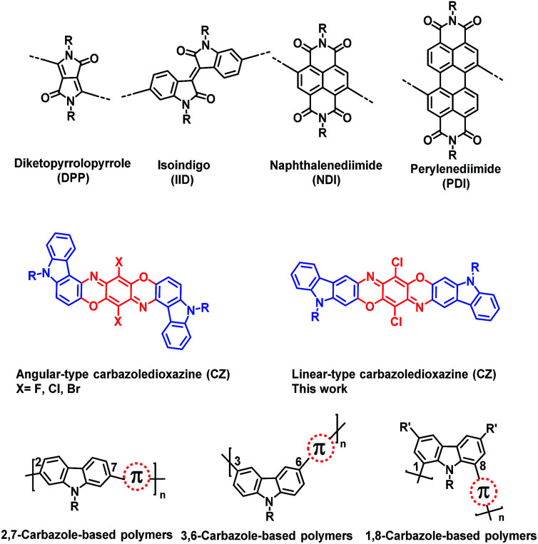
We report the synthesis of a linear-type dibromocarbazoledioxazine (CZ) derivative as a new precursor for semiconducting polymers. The chemical structures of the CZ unit and its polymers with thiophene or thienothiophene spacers (namely, PCZT and PCZTT) were fully characterized. PCZT and PCZTT possessed similar medium optical band gap (E opt g) and electrochemical band gap (E cv g) of around 1.70 eV estimated from the onset absorption and electrochemical redox potentials of the thin films, respectively. Computational density functional theory (DFT) calculations suggested that the backbone of the PCZT might be highly twisted, while that of PCZTT could be very planar. The effect of different backbone geometries on the charge-transport properties was studied by using thin film transistors (TFTs). The TFT device based on PCZTT showed a four times higher hole mobility as compared to that based on PCZT. The superior TFT performances of PCZTT were reasonably attributed to its edge-on backbone packing orientations toward the Si substrate revealed by the grazing-incidence wide-angle X-ray scattering (GIWAXS), which was favorable for in-plane charge transport in the TFT devices.
This journal is © The Royal Society of Chemistry.
Conflict of interest statement
There are no conflicts to declare.
Figures


Similar articles
-
Thin film structure of tetraceno[2,3-b]thiophene characterized by grazing incidence X-ray scattering and near-edge X-ray absorption fine structure analysis.J Am Chem Soc. 2008 Mar 19;130(11):3502-8. doi: 10.1021/ja0773002. Epub 2008 Feb 23. J Am Chem Soc. 2008. PMID: 18293975
-
Observation of a distinct surface molecular orientation in films of a high mobility conjugated polymer.J Am Chem Soc. 2013 Jan 23;135(3):1092-101. doi: 10.1021/ja310240q. Epub 2013 Jan 11. J Am Chem Soc. 2013. PMID: 23311537
-
Design, synthesis, and characterization of ladder-type molecules and polymers. Air-stable, solution-processable n-channel and ambipolar semiconductors for thin-film transistors via experiment and theory.J Am Chem Soc. 2009 Apr 22;131(15):5586-608. doi: 10.1021/ja809555c. J Am Chem Soc. 2009. PMID: 19331320
-
The Chemistry and Applications of Heteroisoindigo Units as Enabling Links for Semiconducting Materials.Acc Chem Res. 2020 Dec 15;53(12):2855-2868. doi: 10.1021/acs.accounts.0c00480. Epub 2020 Nov 17. Acc Chem Res. 2020. PMID: 33201668
-
Thiophene-Based Organic Semiconductors.Top Curr Chem (Cham). 2017 Oct 24;375(6):84. doi: 10.1007/s41061-017-0174-z. Top Curr Chem (Cham). 2017. PMID: 29063993 Review.
References
-
- Li X. Wang H. Schneider J. A. Wei Z. Lai W. Huang W. Wudl F. Zheng Y. J. Mater. Chem. C. 2017;5:2781–2785. doi: 10.1039/C7TC00263G. - DOI
-
- Cai Y. Zhang X. Xue X. Wei D. Huo L. Sun Y. J. Mater. Chem. C. 2017;5:7777–7783. doi: 10.1039/C7TC01909B. - DOI
-
- Wang Y. Liu Y. Chen S. Peng R. Ge Z. Chem. Mater. 2013;25:3196–3204. doi: 10.1021/cm401618h. - DOI
-
- Wang Y. Yang F. Liu Y. Peng R. Chen S. Ge Z. Macromolecules. 2013;46:1368–1375. doi: 10.1021/ma3025738. - DOI
-
- Wang Y. Klein M. F. G. Hiyoshi J. Kawauchi S. Wong W. W. H. Michinobu T. J. Photopolym. Sci. Technol. 2015;28:385–391. doi: 10.2494/photopolymer.28.385. - DOI
LinkOut - more resources
Full Text Sources
Miscellaneous