. 2022 May 11;13(1):2610.
doi: 10.1038/s41467-022-30335-2.

Diamond mirrors for high-power continuous-wave lasers

Affiliations

Diamond mirrors for high-power continuous-wave lasers

Haig A Atikian et al. Nat Commun. .

Abstract

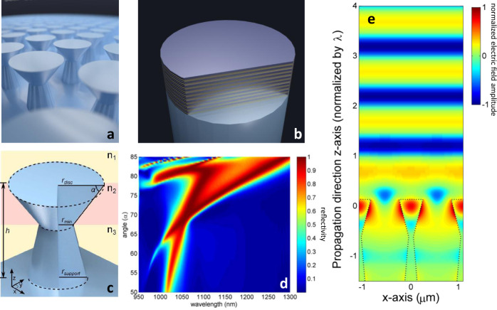
High-power continuous-wave (CW) lasers are used in a variety of areas including industry, medicine, communications, and defense. Yet, conventional optics, which are based on multi-layer coatings, are damaged when illuminated by high-power CW laser light, primarily due to thermal loading. This hampers the effectiveness, restricts the scope and utility, and raises the cost and complexity of high-power CW laser applications. Here we demonstrate monolithic and highly reflective mirrors that operate under high-power CW laser irradiation without damage. In contrast to conventional mirrors, ours are realized by etching nanostructures into the surface of single-crystal diamond, a material with exceptional optical and thermal properties. We measure reflectivities of greater than 98% and demonstrate damage-free operation using 10 kW of CW laser light at 1070 nm, focused to a spot of 750 μm diameter. In contrast, we observe damage to a conventional dielectric mirror when illuminated by the same beam. Our results initiate a new category of optics that operate under extreme conditions, which has potential to improve or create new applications of high-power lasers.


Conflict of interest statement

H.A. and M.L are inventors on patent applications related to this work (U.S. No.: 10,727,072, date filed: May 2016, granted: Jul 2020) and (U.S. Application No.: 15/759,909, date filed: Sept 2016). The authors declare that they have no other competing interests.

Figures

Fig. 1
Fig. 1. Design and simulation of a mirror in single-crystal diamond.
a Graphical depiction of a diamond mirror with the “golf tee”-shaped columns arranged in a hexagonal lattice. b Typical multilayered optical coating deposited onto a substrate. c Schematic of the “golf tee” columns that comprise the diamond mirror, with all relevant dimensions labeled: angle α, radii rdisc, rmin, rsupport, and total height h. The shaded yellow region labeled n1 is of lowest refractive index (air), the red region n2 contains the top portion of the column that features optical resonances and is of highest refractive index, while the yellow region n3 is of lower refractive index and supports the top portion of the column. d Diamond mirror reflection spectrum at normal incidence for varying design angles α, with rdisc = 250 nm, rmin = 50 nm, rsupport = 250 nm, pitch 1.1 μm, and h = 3 μm. Colors indicate reflectivity. e Standing-wave pattern illustrating the reflected wavefront from a diamond mirror at a wavelength of 1064 nm. Mode is confined in the top portion of the columns due to lattice resonance. Colors indicate the electric field amplitude. Photo credit for panels (a) and (b): P. Latawiec, Harvard.
Fig. 2
Fig. 2. Diamond surface fabrication and images.
a Schematic of the reactive ion beam angled etching (RIBAE) fabrication process. (i) Etch mask is patterned onto the diamond sample surface. (ii) Top-down etch with the sample mounted perpendicular to the ion beam path on a rotating sample stage. (iii) Sample is tilted during etching to obtain the target angle α with respect to the direction of the ion beam, uniformly etching underneath the etch mask. (iv) Mask removal yields an array of 3-D nanostructures etched into the surface of diamond. b Optical image of the diamond mirror on a 4.2 mm × 4.2 mm diamond crystal. Each division on the ruler is 1 mm. Photo Credit: H. A. Atikian, Harvard. c SEM image of the diamond mirror taken at 60° from normal. d Zoomed SEM image of the mirror taken at 40° from normal.
Fig. 3
Fig. 3. Optical characterization of a diamond mirror.
a Reflection spectrum of a diamond mirror, blue line is measurement data and red line is FDTD simulation. Absolute reflectivity of 98.9 ± 0.3% is measured at 1064 nm using a DBR laser. Inset shows a zoom-in of the measured spectrum around its maximum. b Beam profile measurement taken of the reflection from the diamond mirror using a scanning-slit profiler. Axes show cross sections of the reflected beam (black circles) with overlaid Gaussian fit (red). Fit yields a 4σ beam width of ~1.5 mm. Distance refers to the amount traveled by the slit relative to its initial position. Inset shows a 3-D perspective of the reflected beam, with axes (and its units) identical to the main figure. Colors indicate normalized optical intensity.
Fig. 4
Fig. 4. Laser-induced damage testing of diamond and dielectric mirrors.
a Optical image of a diamond mirror mounted on a water-cooled stage that was taken prior to testing. be Thermal images of the diamond mirror irradiated by 0.5, 2.5, 5, and 10 kW, respectively, of continuous-wave laser power. Color bar shows the temperature of the setup with varying scale for each image. Temperature accuracy is ±2°. Hot spot corresponds to the position of the beam (on the diamond mirror). At increased power levels a small fraction of optical power leaking through the backside of the diamond mirror results in heating of the stage. f Wide-area SEM image of the diamond mirror shows no damage after testing. Scale bar is 5 μm. g Optical image of a corresponding dielectric mirror mounted on the water-cooled stage. hk Thermal images of the dielectric mirror irradiated by 0.5, 2, 6, and 10 kW, respectively, of CW laser power. Damage ensues at 10 kW of power due to thermal stress. l Image of damage region of dielectric mirror taken after testing shows a several mm-sized hole where the laser beam ablated the dielectric. Photo Credit for panels (a), (g) and (l): S. DeFrances, Penn State EOC.
Fig. 5
Fig. 5. Reactive ion beam etching (RIBAE).
a Graphical depiction of RIBAE. b RIBAE fabrication steps (i) Top-down etching of a diamond sample mounted perpendicular to the ion beam path on a rotating sample stage. (ii) Sample is tilted to obtain an acute angle between the sample and ion beam, uniformly etching underneath the etch mask. (iii) Mask removal yields undercut nanostructures from a bulk substrate.
Fig. 6
Fig. 6. Schematic of the experimental setup used for measuring the reflection spectrum of a diamond mirror and beam profile measurements.
The reflection spectrum is measured using light from a 1065 nm SLD that is collimated and directed with broadband silver mirrors to a 50:50 beamsplitter after passing through a focusing lens. Reflected light from the diamond mirror, or a reference mirror, is directed to an optical spectrum analyzer (OSA) after passing through a defocusing lens. A 1064 nm DBR laser source and free-space optical photodetector (PD) replaced the diode and OSA for the more precise reflectivity measurements. The PD was replaced by a scanning slit profiler (SSP) for beam profile measurements.
Fig. 7
Fig. 7. Reflection spectrum of the diamond mirror used for LIDT measurements at 1070 nm.
A diamond mirror measured (blue curve) and simulated (red curve) reflection spectrum at normal incidence. Green curve shows the spectrum of the 10 kW IPG laser used during damage testing plotted in arbitrary units.
Fig. 8
Fig. 8. Beam profile of 1070 nm IPG LIDT test laser.
Beam profile is collected using a Primes focus monitor. The focus monitor has a metal tip with a 20 μm-diameter pinhole in the side. The rotating tip then traverses the entire area of the beam, collecting 2-D data of the beam profile. Blue line represents the raw data from the x-axis of the beam. The blue (red) line is the data (Gaussian fit).

References

    1. Nilsson J, Payne DN. High-power fiber lasers. Science. 2011;332:921–922. doi: 10.1126/science.1194863. - DOI - PubMed
    1. Jackson SD. Towards high-power mid-infrared emission from a fibre laser. Nat. Photonics. 2012;6(7):423–431. doi: 10.1038/nphoton.2012.149. - DOI
    1. Crafer, R. & Oakley, P. J. Laser processing in manufacturing. Springer (2013).
    1. Katayama, S. ed. Handbook of laser welding technologies. Elsevier (2013).
    1. Martin JH, et al. 3D printing of high-strength aluminium alloys. Nature. 2017;549(7672):365–369. doi: 10.1038/nature23894. - DOI - PubMed