

Band offset and an ultra-fast response UV-VIS photodetector in γ-In2Se3/p-Si heterojunction heterostructures
- PMID: 35547303
- PMCID: PMC9085293
- DOI: 10.1039/c8ra05677c
Band offset and an ultra-fast response UV-VIS photodetector in γ-In2Se3/p-Si heterojunction heterostructures
Abstract
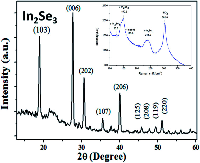
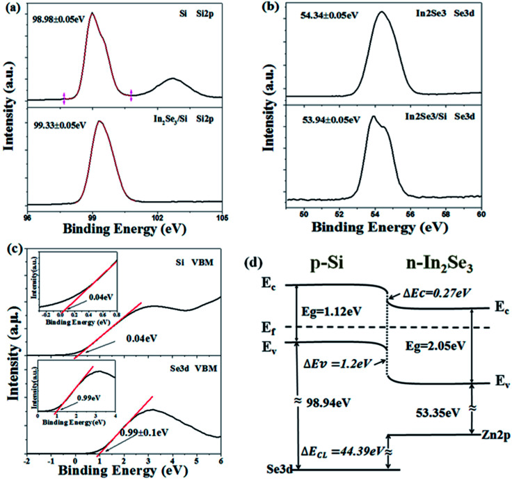
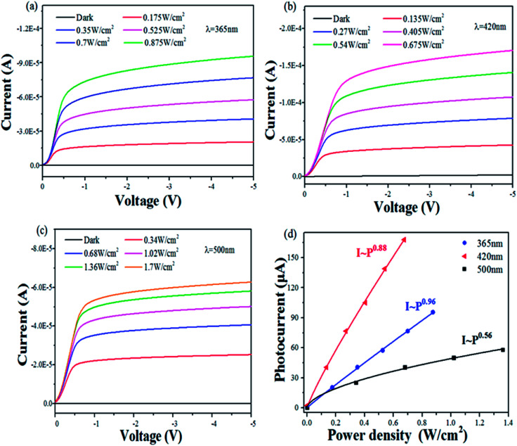
High-quality γ-In2Se3 thin films and a γ-In2Se3/p-Si heterojunction were prepared using pulse laser deposition (PLD). The band offset of this heterojunction was studied by XPS and the band structure was found to be type II structure. The valence band offset (ΔE v) and the conduction band offset (ΔE c) of the heterojunction were determined to be 1.2 ± 0.1 eV and 0.27 ± 0.1 eV, respectively. The γ-In2Se3/p-Si heterojunction photodetector has high responsivity under UV to visible light illumination. The heterojunction exhibits highly stable photodetection characteristics with an ultrafast response/recovery time of 15/366 μs. The ultrafast response time was attributed to type II structure band alignment, which was good for the separation of electron-hole pairs and it can quickly reduce recombination. These excellent properties make γ-In2Se3/p-Si heterojunctions a promising candidate for photodetector applications.
This journal is © The Royal Society of Chemistry.
Conflict of interest statement
There are no conflicts to declare.
Figures


Similar articles
-
Self-powered γ-In2Se3/p-Si heterojunction for photodetection: exploring humidity and light intensity dependent photoresponse.Opt Express. 2024 Oct 21;32(22):38258-38274. doi: 10.1364/OE.531354. Opt Express. 2024. PMID: 39573673
-
Catalyst-free growth of dense γ-In2Se3 nanosheet arrays and their application in photoelectric detectors.Nanotechnology. 2020 May 8;31(19):195601. doi: 10.1088/1361-6528/ab674a. Epub 2020 Jan 3. Nanotechnology. 2020. PMID: 31899909
-
Self-Assembly of the Lateral In2Se3/CuInSe2 Heterojunction for Enhanced Photodetection.ACS Appl Mater Interfaces. 2017 Mar 1;9(8):7288-7296. doi: 10.1021/acsami.6b16323. Epub 2017 Feb 16. ACS Appl Mater Interfaces. 2017. PMID: 28181796
-
Ferroelectrically Modulated and Enhanced Photoresponse in a Self-Powered α-In2Se3/Si Heterojunction Photodetector.ACS Nano. 2023 Apr 11;17(7):6534-6544. doi: 10.1021/acsnano.2c11925. Epub 2023 Mar 23. ACS Nano. 2023. PMID: 36952315 Free PMC article.
-
Self-Assembly High-Performance UV-vis-NIR Broadband β-In2Se3/Si Photodetector Array for Weak Signal Detection.ACS Appl Mater Interfaces. 2017 Dec 20;9(50):43830-43837. doi: 10.1021/acsami.7b16329. Epub 2017 Dec 11. ACS Appl Mater Interfaces. 2017. PMID: 29192488
Cited by
-
Field induced crossover in critical behaviour and direct measurement of the magnetocaloric properties of La0.4Pr0.3Ca0.1Sr0.2MnO3.Sci Rep. 2020 Nov 10;10(1):19485. doi: 10.1038/s41598-020-76321-w. Sci Rep. 2020. PMID: 33173113 Free PMC article.
References
LinkOut - more resources
Full Text Sources