

Inversion domain boundaries in MoSe2 layers
- PMID: 35548164
- PMCID: PMC9086446
- DOI: 10.1039/c8ra07205a
Inversion domain boundaries in MoSe2 layers
Abstract
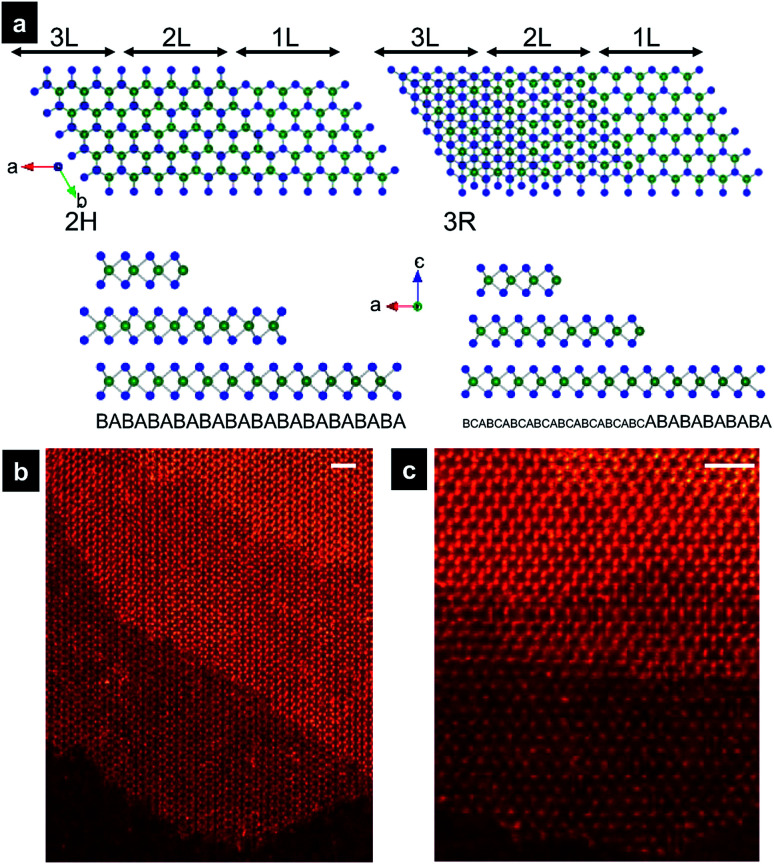
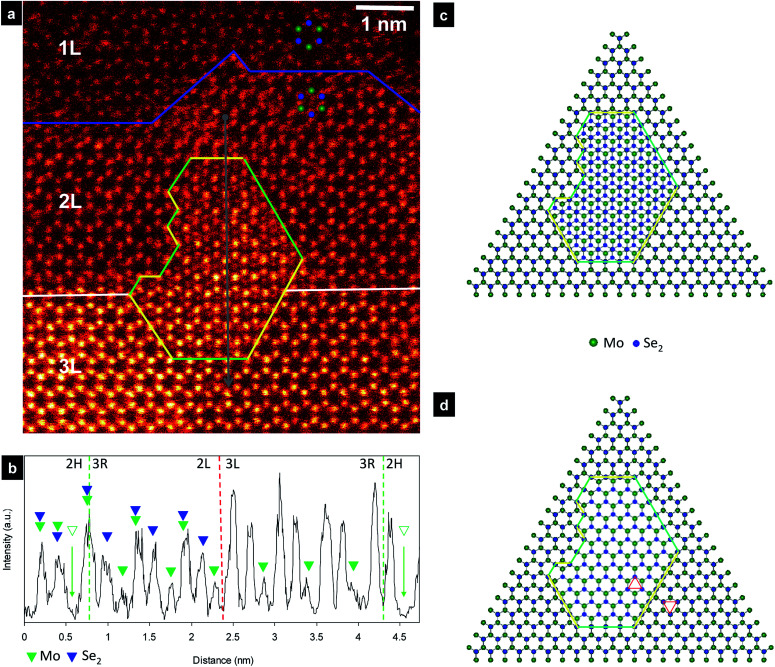
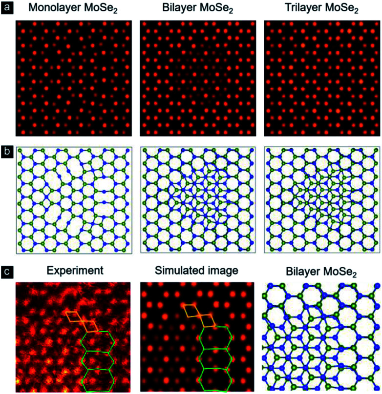
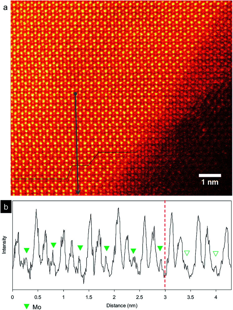
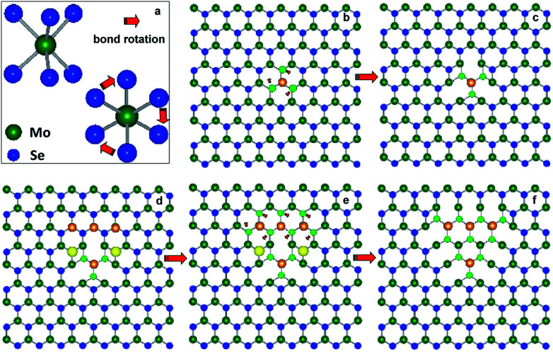
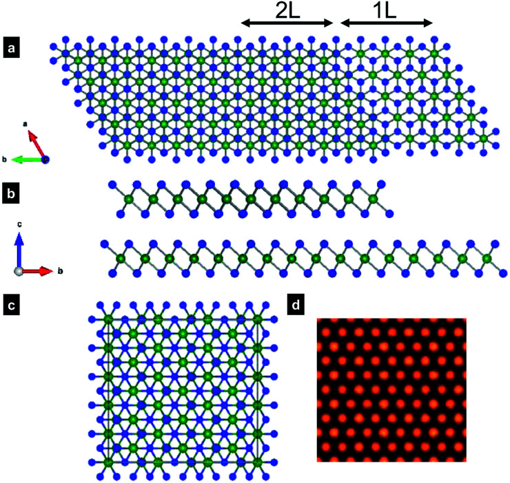
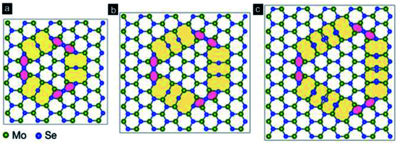
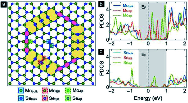
Structural defects, including point defects, dislocation and planar defects, significantly affect the physical and chemical properties of low-dimensional materials, such as layered compounds. In particular, inversion domain boundary is an intrinsic defect surrounded by a 60° grain boundary, which significantly influences electronic transport properties. We study atomic structures of the inversion domain grain boundaries (IDBs) in layered transition metal dichalcogenides (MoSe2 and MoS2) obtained by an exfoliation method, based on the aberration-corrected scanning transmission electron microscopy observation and density functional theory (DFT) calculation. The atomic-scale observation shows that the grain boundaries consist of two different types of 4-fold ring point shared and 8-fold ring edge shared chains. The results of DFT calculations indicate that the inversion domain grain boundary behaves as a metallic one-dimensional chain embedded in the semiconducting MoSe2 matrix with the occurrence of a new state within the band gap.
This journal is © The Royal Society of Chemistry.
Conflict of interest statement
There is no conflicts of interest to declare.
Figures
Similar articles
-
Metallic Twin Grain Boundaries Embedded in MoSe2 Monolayers Grown by Molecular Beam Epitaxy.ACS Nano. 2017 May 23;11(5):5130-5139. doi: 10.1021/acsnano.7b02172. Epub 2017 May 1. ACS Nano. 2017. PMID: 28453936
-
Intrinsic structural defects in monolayer molybdenum disulfide.Nano Lett. 2013 Jun 12;13(6):2615-22. doi: 10.1021/nl4007479. Epub 2013 May 9. Nano Lett. 2013. PMID: 23659662
-
Synthesis and defect investigation of two-dimensional molybdenum disulfide atomic layers.Acc Chem Res. 2015 Jan 20;48(1):31-40. doi: 10.1021/ar500291j. Epub 2014 Dec 9. Acc Chem Res. 2015. PMID: 25490347
-
Grain boundary atomic structures and light-element visualization in ceramics: combination of Cs-corrected scanning transmission electron microscopy and first-principles calculations.J Electron Microsc (Tokyo). 2011;60 Suppl 1:S173-88. doi: 10.1093/jmicro/dfr049. J Electron Microsc (Tokyo). 2011. PMID: 21844588 Review.
-
Atomic structure of defects and dopants in 2D layered transition metal dichalcogenides.Chem Soc Rev. 2018 Aug 28;47(17):6764-6794. doi: 10.1039/c8cs00236c. Chem Soc Rev. 2018. PMID: 29974919 Review.
Cited by
-
Chemical Vapor Deposition Mediated Phase Engineering for 2D Transition Metal Dichalcogenides: Strategies and Applications.Small Sci. 2021 Oct 19;2(1):2100047. doi: 10.1002/smsc.202100047. eCollection 2022 Jan. Small Sci. 2021. PMID: 40212328 Free PMC article.
References
LinkOut - more resources
Full Text Sources
Miscellaneous