. 2022 May 12;12(1):7884.
doi: 10.1038/s41598-022-11610-0.

Super strong wide TM Mie bandgaps tolerating disorders

Affiliations

Super strong wide TM Mie bandgaps tolerating disorders

Kiyanoush Goudarzi et al. Sci Rep. .

Abstract

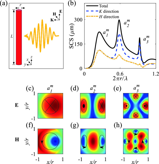
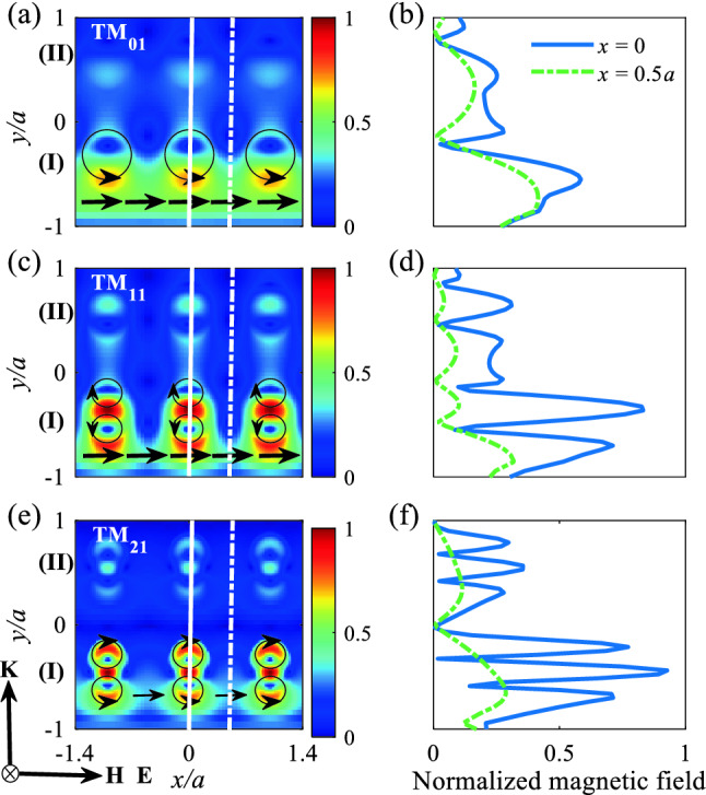
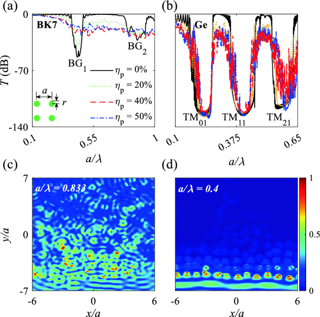
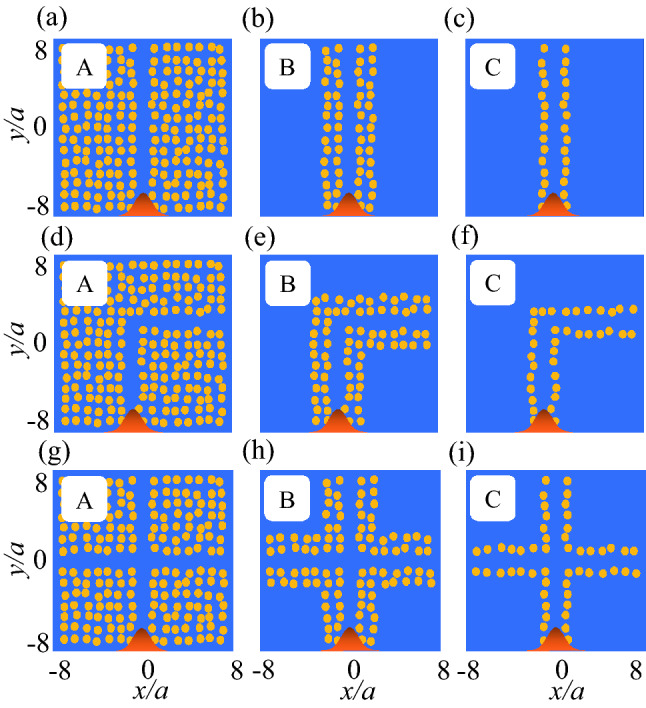
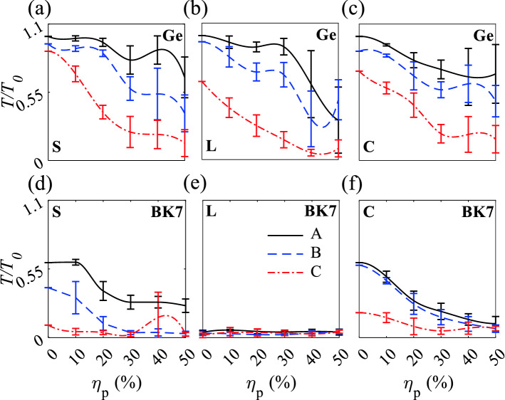
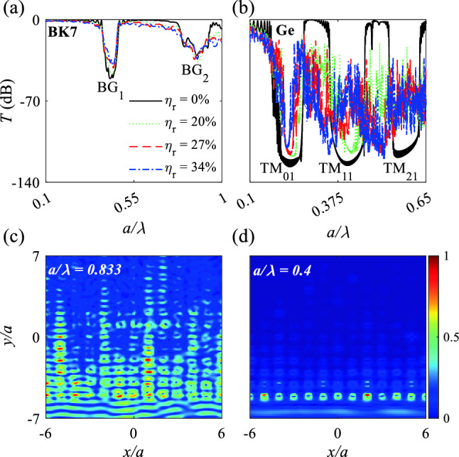
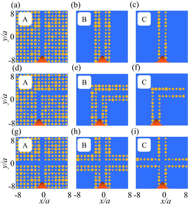
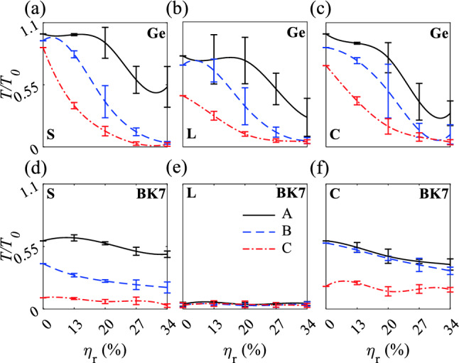
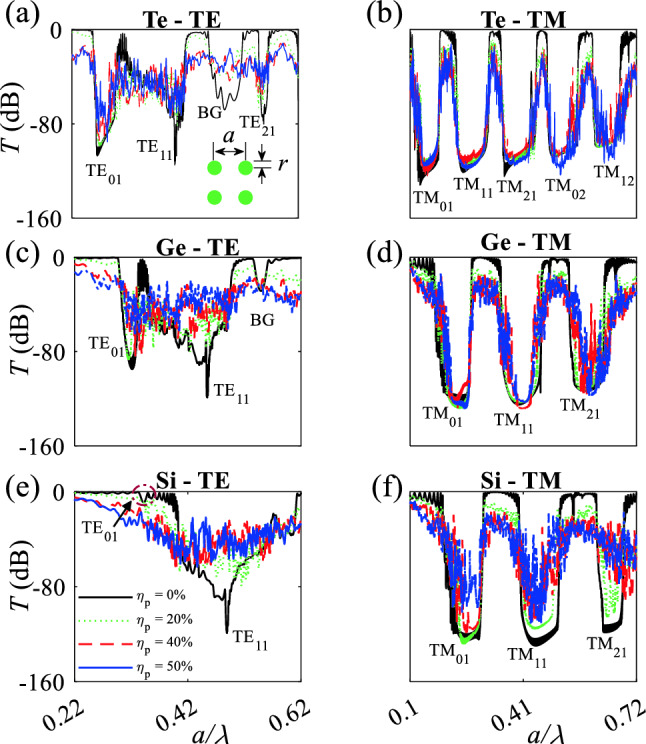
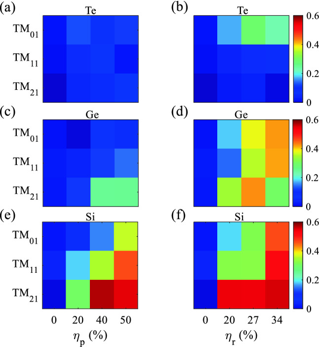
This study demonstrates the appearance of super intense and wide Mie bandgaps in metamaterials composed of tellurium, germanium, and silicon rods in air that tolerate some disordering of rod position and rod radius under transverse magnetic (TM) polarized light waves. Tellurium metamaterials reveal [Formula: see text], [Formula: see text], [Formula: see text], [Formula: see text], [Formula: see text] Mie bandgap modes in which [Formula: see text], [Formula: see text], and [Formula: see text] tolerate high rod-position disordering of [Formula: see text] and rod-radius disordering of 34 and [Formula: see text], respectively. Results for germanium metamaterials show Mie bandgap modes [Formula: see text], [Formula: see text], and [Formula: see text], in which [Formula: see text] and [Formula: see text] tolerate rod-position disordering of [Formula: see text], and rod-radius disordering of 34 and [Formula: see text], respectively. Using these characteristics of [Formula: see text] in germanium metamaterials under position and radius disordering, ultra-narrow straight, L-shaped, and crossing waveguides that contain 14, four, and two rows of germanium rods in air are designed. Also, it is shown that [Formula: see text] Mie bandgap appears in metamaterials containing a high refractive index, and disappears in metamaterials with a lower refractive index such as silicon; in contrast, a new phenomenon of intense and broadband [Formula: see text], [Formula: see text], and [Formula: see text] in metamaterials with a lower refractive index such as silicon appear. In silicon-based metamaterials, [Formula: see text] tolerates high rod-position and rod-radius disordering of [Formula: see text] and [Formula: see text], respectively, and [Formula: see text] shows robustness to rod-position and rod-radius disordering of [Formula: see text]. This strong tolerance of disordering of TM modes in tellurium, germanium, and silicon metamaterials opens a new way to design small, high-efficient, and feasible fabrication optical devices for optical integrated circuits.


Conflict of interest statement

The authors declare no competing interests.

Figures

Figure 1
Figure 1
(a) Illumination of a single Ge rod with a refractive index n = 4, radius r, and length L (Lr) under a TM polarized plane wave (electric field along the long axis). (b) SCS of a long single Ge rod under TM polarized plane wave versus normalized frequency. (ce) and (fh) show E- and H-field distributions, respectively, of the rod for the Mie resonances of a1m, a2m, and a3m. Blue to red show minimum to maximum of the fields.
Figure 2
Figure 2
Periodic arrays of Ge rods in air under excitation of (a) TM01, (c) TM11 and (e) TM21 Mie bandgaps. (b), (d) and (f) Normalized magnetic fields for (a), (c), and (e), respectively, over y axis for two lines of x=0 and x=0.5a. Incident plane has been located at the bottom of the structure and propagates from -y to y direction. Black arrows represent the direction of magnetic fields.
Figure 3
Figure 3
(a) and (b) logarithmic transmission spectra of BK7 PCs and Ge MMs in a cubic pattern under TM polarized plane waves (H field along x direction) for position disordering ηp = 0, 20, 40, and 50%. (c) and (d) H-field distributions of BK7 PCs and Ge MMs at the center of the Bragg bandgap BG2 (aλ=0.833) and Mie bandgap TM11 (aλ=0.41) under ηp = 40%. The plane waves propagate from -y to y direction.
Figure 4
Figure 4
All-dielectric straight, L-shaped, and crossing waveguides surrounded by (a), (d), and (g) 14, (b), (e), and (h) four, and (c), (f), and (i) two rows of dielectric rods in air that are called A, B, and C structures. The dielectric rods are either BK7 or Ge. The waveguides are under ηp=20%. Yellow: dielectric rod; blue: air. An incident Gaussian sources located at the bottom of the structures and propagate from -y to y direction.
Figure 5
Figure 5
Normalized transmission versus ηp for A, B, and C straight, L-shaped, and crossing waveguides. (a)–(c) and (d)–(f) Ge and BK7 waveguides. Gaussian sources are lunched at the bottom of the waveguides, propagate from -y to y direction. S, L, and C stand for straight, L-shaped and crossing waveguides, respectively.
Figure 6
Figure 6
(a) and (b) logarithmic transmission spectra of BK7 PCs and Ge MMs in a cubic pattern under TM polarized plane waves (H field along x direction) for radius disordering ηr = 0, 20, 27, and 34%. (c) and (d) H-field distributions of BK7 PCs and Ge MMs at the center of the Bragg bandgap BG2 (aλ=0.833) and Mie bandgap TM11 (aλ=0.41) under ηr = 27%. The plane waves propagate from -y to y.
Figure 7
Figure 7
All-dielectric straight, L-shaped, and crossing waveguides surrounded by (a), (d), and (g) 14, (b), (e), and (h) four, and (c), (f), and (i) two rows of dielectric rods in air that are called A, B, and C structures. The waveguides are under ηr=27%. The dielectric rods are either BK7 or Ge. Yellow: dielectric rod; blue: air. An incident Gaussian sources located at the bottom of the structures and propagate from -y to y direction.
Figure 8
Figure 8
Normalized transmission versus ηr for A, B, and C straight, L-shaped, and crossing waveguides. (a)–(c) and (d)–(f) Ge and BK7 waveguides. Gaussian sources are lunched at the bottom of the waveguides, propagate from -y to y direction. S, L, and C stand for straight, L-shaped and crossing waveguides, rspectively.
Figure 9
Figure 9
Logarithmic transmission spectra of Te MMs contain 15×15 Te rods in air under illumination of TE (a) and TM (b) plane waves, respectively. The spectra of 15×15 Ge rods in air under illumination of TE (c) and TM (d) plane waves, respectively. (e) and (f) show the spectra of 15×15 Si rods in air under illumination of TE and TM polarized plane waves, respectively. Solid black, dotted green, dashed red, and dot-dashed blue curves represent the position disordering of ηp=0,20,40, and 50%, respectively.
Figure 10
Figure 10
γ parameter for TM01, TM11, and TM21 Mie bandgap modes for the structures contain Te (a), Ge (c), and Si (e) rods in air under rod-position disordering of ηp=0,20,40, and 50%. γ parameter for TM01, TM11, and TM21 Mie bandgap modes for the structures contain Te (b), Ge (d), and Si (f) rods in air under rod-radius disordering of ηr=0,20,27, and 34%.

Similar articles

Cited by

References

    1. Gerislioglu B, et al. Monolithic metal dimer-on-film structure: New plasmonic properties introduced by the underlying metal. Nano Lett. 2020;20:2087–2093. doi: 10.1021/acs.nanolett.0c00075. - DOI - PubMed
    1. Perera T, Gunapala SD, Stockman MI, Premaratne M. Plasmonic properties of metallic nanoshells in the quantum limit: From single particle excitations to plasmons. J. Phys. Chem. C. 2020;124:27694–27708. doi: 10.1021/acs.jpcc.0c10507. - DOI
    1. García-Lojo D, et al. Plasmonic supercrystals. Acc. Chem. Res. 2019;52:1855–1864. doi: 10.1021/acs.accounts.9b00213. - DOI - PubMed
    1. Wang Y, et al. Plasmon resonances of highly doped two-dimensional mos2. Nano Lett. 2015;15:883–890. doi: 10.1021/nl503563g. - DOI - PubMed
    1. Garcĩa-Garcĩa I, et al. Silver-based plasmonic catalysts for carbon dioxide reduction. ACS Sustain. Chem. Eng. 2020;8:1879–1887. doi: 10.1021/acssuschemeng.9b06146. - DOI