

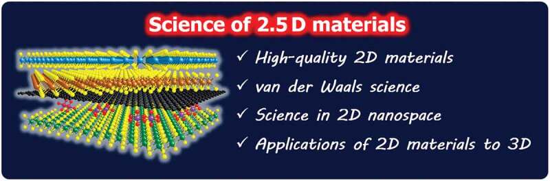
Science of 2.5 dimensional materials: paradigm shift of materials science toward future social innovation
- PMID: 35557511
- PMCID: PMC9090349
- DOI: 10.1080/14686996.2022.2062576
Science of 2.5 dimensional materials: paradigm shift of materials science toward future social innovation
Abstract
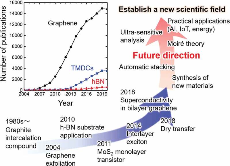
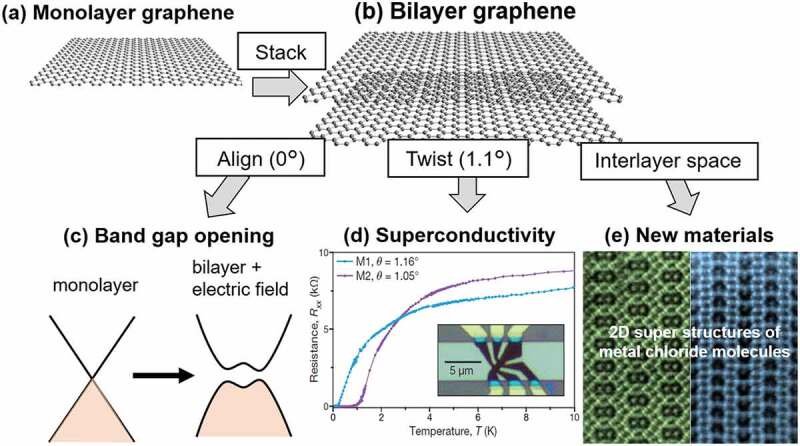
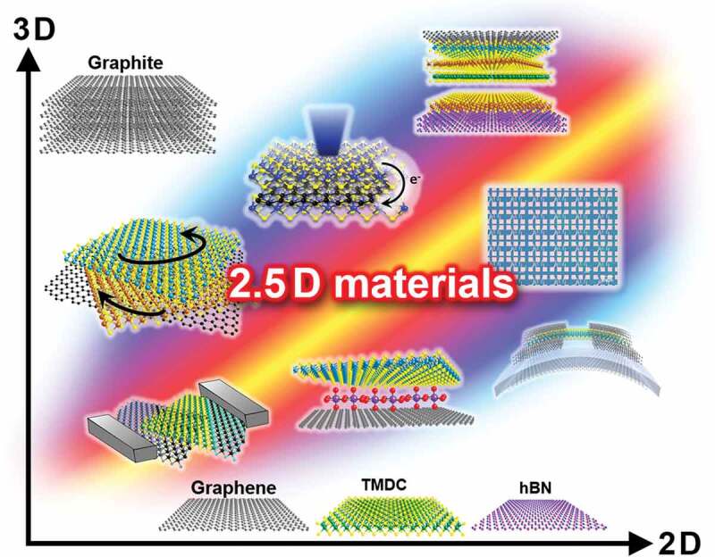
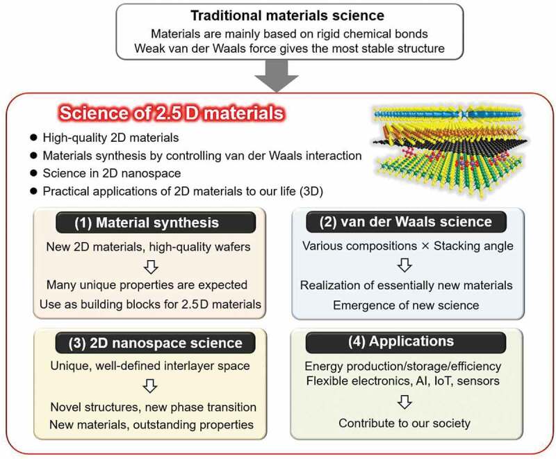
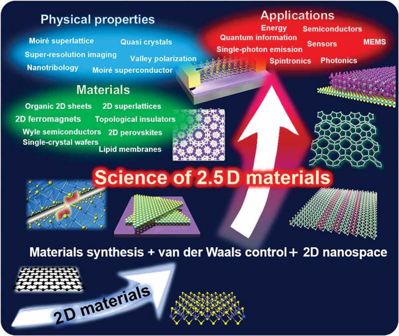
The past decades of materials science discoveries are the basis of our present society - from the foundation of semiconductor devices to the recent development of internet of things (IoT) technologies. These materials science developments have depended mainly on control of rigid chemical bonds, such as covalent and ionic bonds, in organic molecules and polymers, inorganic crystals and thin films. The recent discovery of graphene and other two-dimensional (2D) materials offers a novel approach to synthesizing materials by controlling their weak out-of-plane van der Waals (vdW) interactions. Artificial stacks of different types of 2D materials are a novel concept in materials synthesis, with the stacks not limited by rigid chemical bonds nor by lattice constants. This offers plenty of opportunities to explore new physics, chemistry, and engineering. An often-overlooked characteristic of vdW stacks is the well-defined 2D nanospace between the layers, which provides unique physical phenomena and a rich field for synthesis of novel materials. Applying the science of intercalation compounds to 2D materials provides new insights and expectations about the use of the vdW nanospace. We call this nascent field of science '2.5 dimensional (2.5D) materials,' to acknowledge the important extra degree of freedom beyond 2D materials. 2.5D materials not only offer a new field of scientific research, but also contribute to the development of practical applications, and will lead to future social innovation. In this paper, we introduce the new scientific concept of this science of '2.5D materials' and review recent research developments based on this new scientific concept.
Keywords: 2.5 dimensional materials; 2D heterostructures; bilayer graphene; hexagonal boron nitride; intercalation; interlayer nanospace; moiré superlattice; multidimensional materials; transition metal dichalcogenide; van der Waals interaction.
© 2022 The Author(s). Published by National Institute for Materials Science in partnership with Taylor & Francis Group.
Conflict of interest statement
No potential conflict of interest was reported by the author(s).
Figures
Similar articles
-
Synthesis of hexagonal boron nitride heterostructures for 2D van der Waals electronics.Chem Soc Rev. 2018 Aug 13;47(16):6342-6369. doi: 10.1039/c8cs00450a. Chem Soc Rev. 2018. PMID: 30043784 Review.
-
Recent Advances in Two-Dimensional Materials beyond Graphene.ACS Nano. 2015 Dec 22;9(12):11509-39. doi: 10.1021/acsnano.5b05556. Epub 2015 Nov 24. ACS Nano. 2015. PMID: 26544756
-
Band engineering for novel two-dimensional atomic layers.Small. 2015 Apr 24;11(16):1868-84. doi: 10.1002/smll.201402380. Epub 2014 Dec 15. Small. 2015. PMID: 25510534
-
Epitaxial Intercalation Growth of Scalable Hexagonal Boron Nitride/Graphene Bilayer Moiré Materials with Highly Convergent Interlayer Angles.ACS Nano. 2021 Sep 28;15(9):14384-14393. doi: 10.1021/acsnano.1c03698. Epub 2021 Sep 14. ACS Nano. 2021. PMID: 34519487
-
Precision Intercalation of Organic Molecules in 2D Layered Materials: From Interface Chemistry to Low-Dimensional Physics.Precis Chem. 2025 Jan 10;3(2):51-71. doi: 10.1021/prechem.4c00084. eCollection 2025 Feb 24. Precis Chem. 2025. PMID: 40018453 Free PMC article. Review.
Cited by
-
Band engineering of layered oxyhalide photocatalysts for visible-light water splitting.Chem Sci. 2024 Jun 26;15(30):11719-11736. doi: 10.1039/d4sc02093f. eCollection 2024 Jul 31. Chem Sci. 2024. PMID: 39092126 Free PMC article. Review.
-
High-throughput dry transfer and excitonic properties of twisted bilayers based on CVD-grown transition metal dichalcogenides.Nanoscale Adv. 2023 Sep 4;5(18):5115-5121. doi: 10.1039/d3na00371j. eCollection 2023 Sep 12. Nanoscale Adv. 2023. PMID: 37705802 Free PMC article.
-
Low-Dimensional Structures for Smart Materials and Composites: Preparation, Properties and Applications.Materials (Basel). 2023 Aug 22;16(17):5743. doi: 10.3390/ma16175743. Materials (Basel). 2023. PMID: 37687433 Free PMC article.
-
Unravelling the formation of carbyne nanocrystals from graphene nanoconstrictions through the hydrothermal treatment of agro-industrial waste molasses.Nanoscale Adv. 2024 Mar 28;6(9):2390-2406. doi: 10.1039/d4na00076e. eCollection 2024 Apr 30. Nanoscale Adv. 2024. PMID: 38694474 Free PMC article.
-
Flaw-size-dependent mechanical interlayer coupling and edge-reconstruction embrittlement in van der Waals materials.Nat Mater. 2025 Mar 28. doi: 10.1038/s41563-025-02194-x. Online ahead of print. Nat Mater. 2025. PMID: 40155557
References
-
- Novoselov KS, Geim AK, Morozov SV, et al. Electric field effect in atomically thin carbon films. Science. 2004;306:666–669. - PubMed
-
- Geim AK, Novoselov KS.. The rise of graphene. Nat Mater. 2007;6:183–191. - PubMed
-
- Zurutuza A, Marinelli C.. Challenges and opportunities in graphene commercialization. Nat Nanotechnol. 2014;9:730–734. - PubMed
-
- Choi W, Choudhary N, Han GH, et al. Recent development of two-dimensional transition metal dichalcogenides and their applications. Mater Today. 2017;20:116–130.
-
- Mannix AJ, Kiraly B, Hersam MC, et al. Synthesis and chemistry of elemental 2D materials. Nat Rev Chem. 2017;1:0014.
Publication types
LinkOut - more resources
Full Text Sources
Miscellaneous