Review
. 2022 May 6;12(9):1582.
doi: 10.3390/nano12091582.

Theory of Excitons in Atomically Thin Semiconductors: Tight-Binding Approach

Affiliations
Review

Theory of Excitons in Atomically Thin Semiconductors: Tight-Binding Approach

Maciej Bieniek et al. Nanomaterials (Basel). .

Abstract

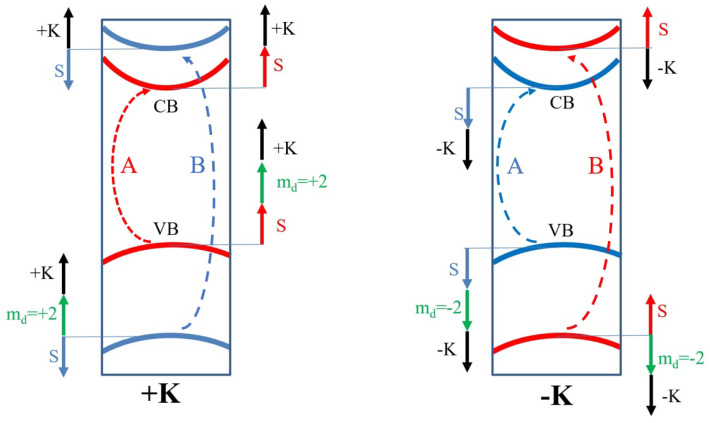
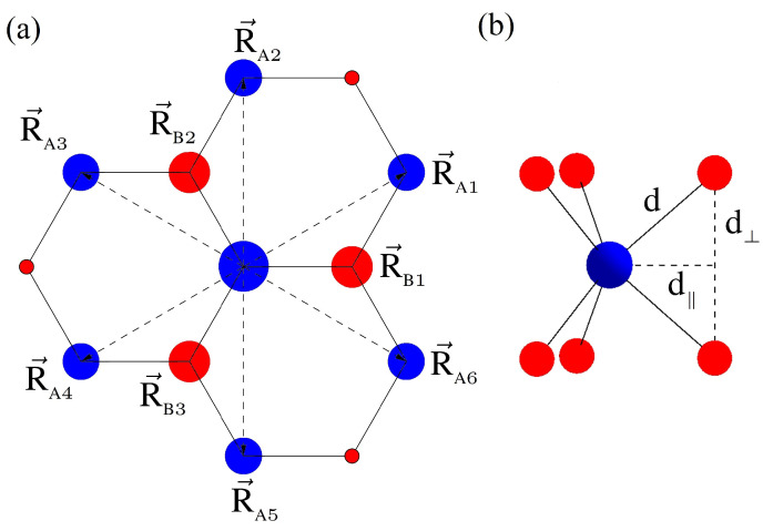
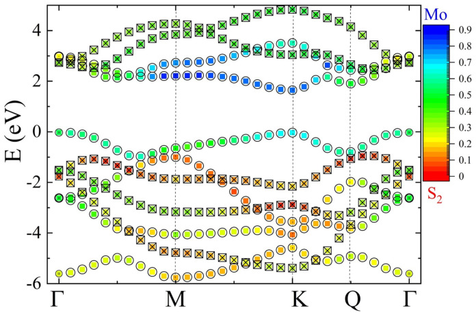
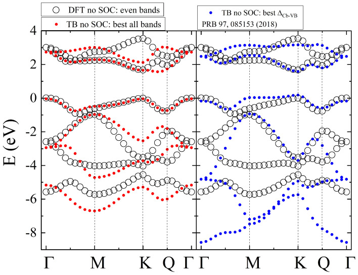
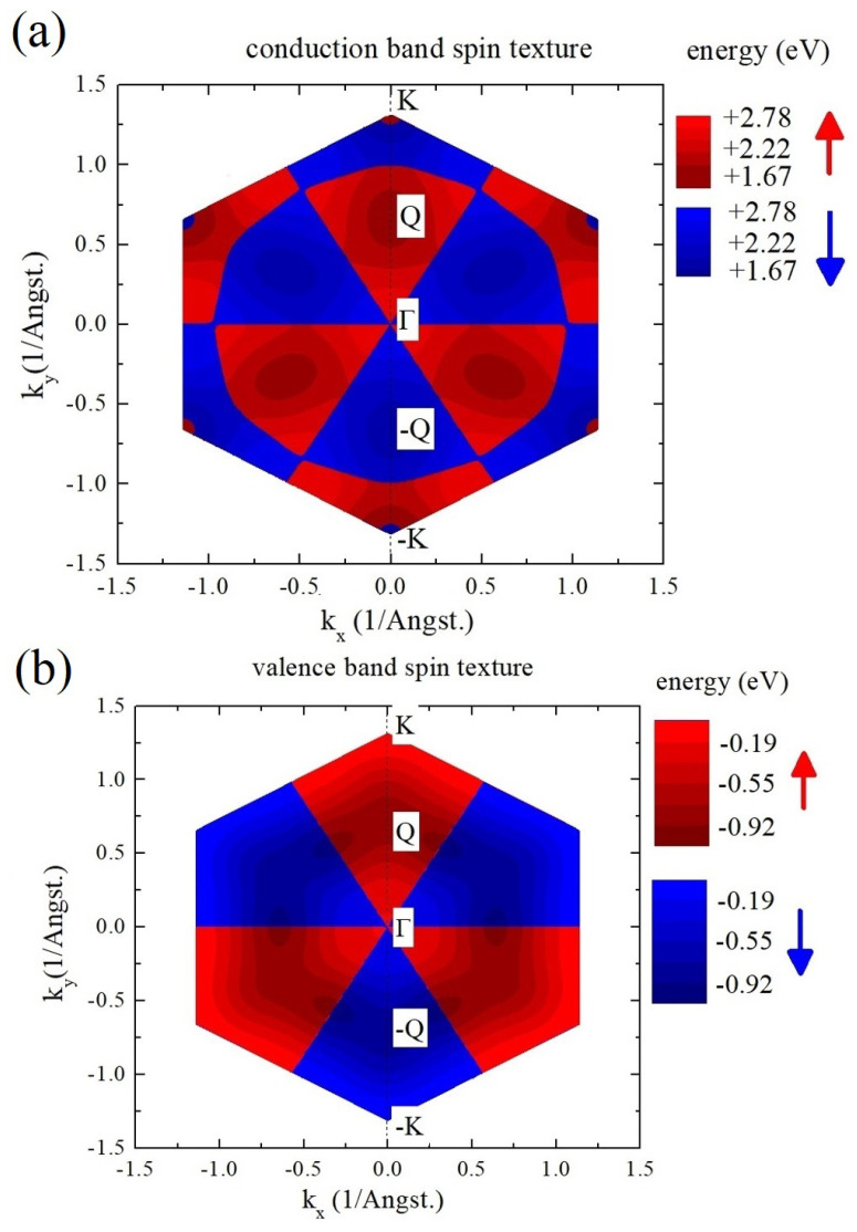
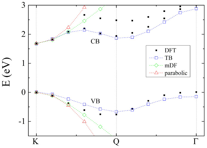
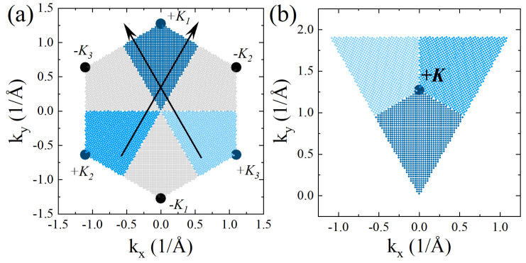
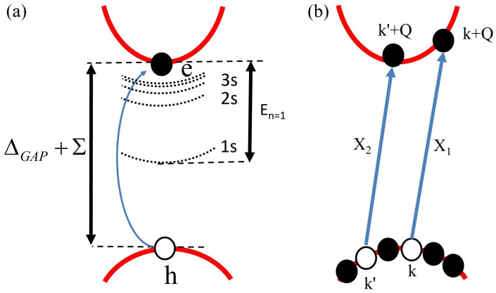
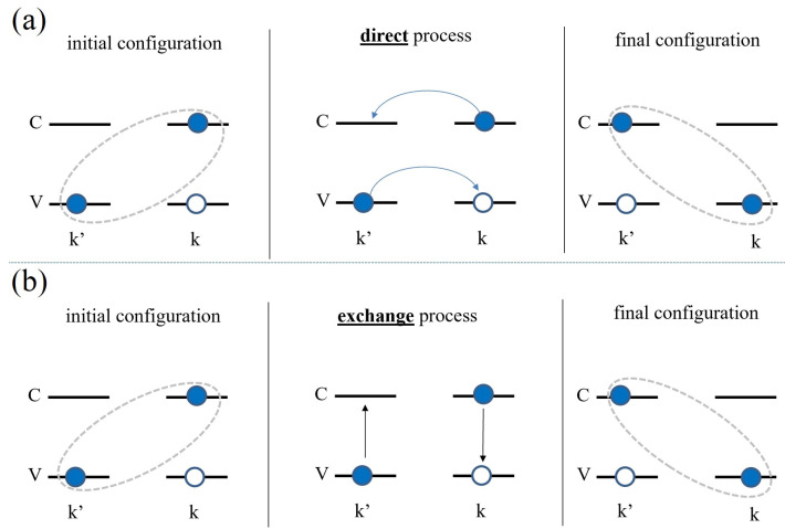
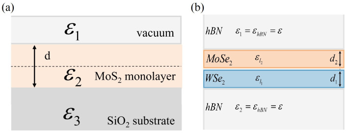
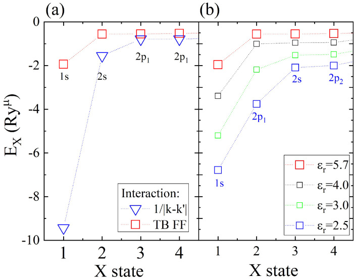
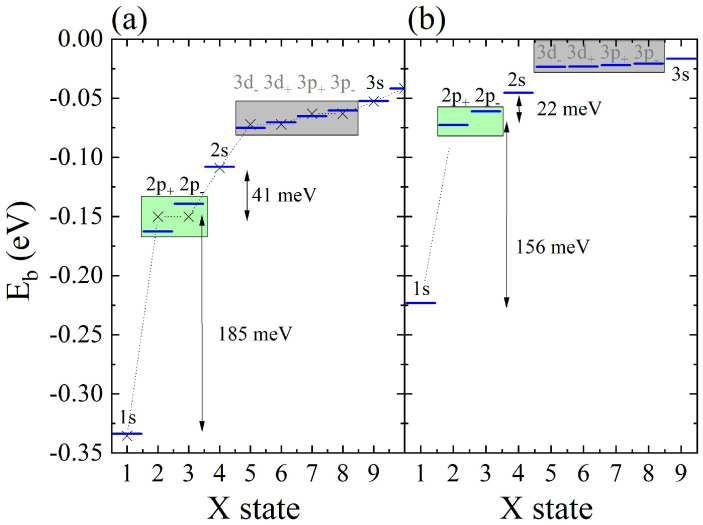
Atomically thin semiconductors from the transition metal dichalcogenide family are materials in which the optical response is dominated by strongly bound excitonic complexes. Here, we present a theory of excitons in two-dimensional semiconductors using a tight-binding model of the electronic structure. In the first part, we review extensive literature on 2D van der Waals materials, with particular focus on their optical response from both experimental and theoretical points of view. In the second part, we discuss our ab initio calculations of the electronic structure of MoS2, representative of a wide class of materials, and review our minimal tight-binding model, which reproduces low-energy physics around the Fermi level and, at the same time, allows for the understanding of their electronic structure. Next, we describe how electron-hole pair excitations from the mean-field-level ground state are constructed. The electron-electron interactions mix the electron-hole pair excitations, resulting in excitonic wave functions and energies obtained by solving the Bethe-Salpeter equation. This is enabled by the efficient computation of the Coulomb matrix elements optimized for two-dimensional crystals. Next, we discuss non-local screening in various geometries usually used in experiments. We conclude with a discussion of the fine structure and excited excitonic spectra. In particular, we discuss the effect of band nesting on the exciton fine structure; Coulomb interactions; and the topology of the wave functions, screening and dielectric environment. Finally, we follow by adding another layer and discuss excitons in heterostructures built from two-dimensional semiconductors.

Keywords: Bethe–Salpeter equation; excitons; tight-binding; transition metal dichalcogenides.


Conflict of interest statement

The authors declare no conflict of interest.

Figures

Figure 1
Figure 1
Schematic structure of spin-split bands in monolayer MX2+K/K valleys. Respective A/B excitonic transitions are shown as dashed arrows. Additional solid arrows denote different contributions to the +K and K valleys’ responses to magnetic fields. The solid blue and red arrows show the bare electron Zeeman contribution in magnetic field B=(0,0,Bz); the green—the atomic orbital Landé contribution and the black ones—the valley Zeeman contribution.
Figure 2
Figure 2
(a) Top view of the structure of MX2 in the 2H phase: metal atoms are denoted by blue dots, and chalcogen by red ones. (b) Side view of MX2, showing that the atoms are organized into three layers, central metal and two chalcogen, with structural constants parametrized by d and d.
Figure 3
Figure 3
Color-mapped localization of a given k-resolved eigenenergy on Mo and S2 spheres and symmetry of eigenvalues across the Brillouin zone. Circles (crossed rectangles) denote symmetric (anti-symmetric) orbitals with respect to the metal plane.
Figure 4
Figure 4
Left: TB dispersion obtained after optimizing the SK parameters to reproduce all even DFT bands. Right: TB dispersion optimized to reproduce the transition energy between the VB and CB. We note that the former reproduces the VB very well, while the latter one reproduces the CB very well, especially on the KΓ line.
Figure 5
Figure 5
(a) Spin texture of the CB, showing the spin orientation of the lowest CB spin-split band. (b) Corresponding VB spin texture.
Figure 6
Figure 6
Comparison between dispersion models along the KΓ line. DFT dispersion is denoted by black circles, TB by blue rectangles, massive Dirac fermion by green diamonds, and parabolic (effective mass) model by red triangles. The corresponding connecting lines are shown as a guide to the eye.
Figure 7
Figure 7
(a) Choice of +K valley on the whole BZ. (b) Construction of the valley around a single K point.
Figure 8
Figure 8
(a) The single electron–single hole picture (exciton in effective mass approximation) in which interaction creates a spectrum of bound states. (b) Exact picture where the “hole” is created by exciting the electron from the filled ground state in the VB. The exciton is then constructed as a coherent superposition of all possible excitations for a given center-of-mass momentum QCM interacting via the Coulomb interaction.
Figure 9
Figure 9
Graphical representation of two types of interaction between an electron and a hole: (a) direct process (b) exchange process.
Figure 10
Figure 10
(a) Schematic picture of the dielectric environment of the MoS2 monolayer on the SiO2 substrate. (b) Slab model of the MoSe2/WSe2 heterostructure. Each of the MX2 layers with the width d1,2, respectively, is described by the dielectric constant εl1,l2.
Figure 11
Figure 11
The first two shells of the excitonic spectrum with full tight-binding direct interaction form factors. (a) Effect of the form factors compared to FD=1 approximation. (b) Effect of different static screening on the spectrum. On both (a,b), tight-binding energies of electron and hole are used.
Figure 12
Figure 12
Exciton fine structure for the MoS2 monolayer (a) on the SiO2 substrate and (b) encapsulated with hBN, in a full TB model with complex electron–hole interaction included. Results restricted to the first three shells. The topological splitting of 2p, 3p, and 3d states in the excitonic spectrum of the MoS2 layer is presented.
Figure 13
Figure 13
Interlayer exciton fine structure for the MoSe2/WSe2 heterostructure encapsulated with hBN in the EMA, restricted to 1s, 2p, and 2s states. Interlayer A/B/A˜/B˜ exciton types have been distinguished, where A denotes the transition WSe2–MoSe2 spin-up, B transition MoSe2–WSe2 spin-down, A˜ transition MoSe2–WSe2 spin-up, and B˜ transition WSe2–MoSe2 spin-down, respectively.

Similar articles

Cited by

References

    1. Wallace P.R. The Band Theory of Graphite. Phys. Rev. 1947;71:622–634. doi: 10.1103/PhysRev.71.622. - DOI
    1. Connell G., Wilson J., Yoffe A. Effects of pressure and temperature on exciton absorption and band structure of layer crystals: Molybdenum disulphide. J. Phys. Chem. Solids. 1969;30:287–296. doi: 10.1016/0022-3697(69)90310-2. - DOI
    1. Wilson J., Yoffe A. The transition metal dichalcogenides discussion and interpretation of the observed optical, electrical and structural properties. Adv. Phys. 1969;18:193–335. doi: 10.1080/00018736900101307. - DOI
    1. Novoselov K.S., Geim A.K., Morozov S.V., Jiang D., Zhang Y., Dubonos S.V., Grigorieva I.V., Firsov A.A. Electric Field Effect in Atomically Thin Carbon Films. Science. 2004;306:666–669. doi: 10.1126/science.1102896. - DOI - PubMed
    1. Novoselov K.S., Geim A.K., Morozov S.V., Jiang D., Katsnelson M.I., Grigorieva I.V., Dubonos S.V., Firsov A.A. Two-dimensional gas of massless Dirac fermions in graphene. Nature. 2005;438:197–200. doi: 10.1038/nature04233. - DOI - PubMed

LinkOut - more resources