. 2022 Apr 28;7(18):15315-15325.
doi: 10.1021/acsomega.1c05352. eCollection 2022 May 10.

Chemical Solution Deposition of Insulating Yttria Nanolayers as Current Flow Diverter in Superconducting GdBa2Cu3O7-δ Coated Conductors

Affiliations

Chemical Solution Deposition of Insulating Yttria Nanolayers as Current Flow Diverter in Superconducting GdBa2Cu3O7-δ Coated Conductors

Pedro Barusco et al. ACS Omega. .

Abstract

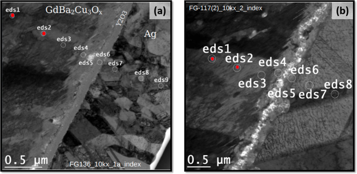
The primary benefit of a metallic stabilization/shunt in high temperature superconductor (HTS) coated conductors (CCs) is to prevent joule heating damage by providing an alternative path for the current flow during the HTS normal state transition (i.e., quench). However, the shunt presence in combination with unavoidable fluctuations in the critical current (I c) of the HTS film can develop a localized quench along the CC's length if the operational current is kept close to I c. This scenario, also known as the hot-spot regime, can lead to the rupture of the CC if the local quench does not propagate fast enough. The current flow diverter (CFD) is the CC architecture concept that has proven to increase the conductor's robustness against a hot-spot regime by simply boosting the quench velocity in the CC, which avoids the shunt compromise in some applications. This work investigates a practical manufacturing route for incorporating the CFD architecture in a reel-to-reel system via the preparation of yttrium oxide (Y2O3) as an insulating thin nanolayer (∼100 nm) on top of a GdBa2Cu3O7 (GdBCO) superconductor. Chemical solution deposition (CSD) using ink jet printing (IJP) is shown to be a suitable manufacturing approach. Two sequences of the experimental steps have been investigated, where oxygenation of the GdBCO layer is performed after or before the solution deposition and the Y2O3 nanolayer thermal treatment formation step. A correlated analysis of the microstructure, in situ oxygenation kinetics, and superconducting properties of the Ag/Y2O3/GdBCO trilayer processed under different conditions shows that a new customized functional CC can be prepared. The successful achievement of the CFD effect in the case of the preoxygenated customized CC was confirmed by measuring the current transfer length, thus demonstrating the effectiveness of the CSD-IJP as a processing method.


Conflict of interest statement

The authors declare no competing financial interest.

Figures

Figure 1
Figure 1
(a) Picture of GdBCO CC after IJP of yttria and pyrolysis at 450 °C. The sample is mounted on a metal plate for silver sputtering. (b) Picture of GdBCO CC after silver sputtering. (c) SEM-FIB cross-section of a THEVA CFD-CC deposited with yttria using ink jet printing.
Figure 2
Figure 2
General schematics of the experimental steps required to produce a yttria nanolayer and realize the CFD architecture. (a) First route: GdBCO layer not oxygenated initially and this step only performed after the yttria CSD process. (b) Second route: Bare GdBCO layer oxygenated first and then CSD and silver coatings done. Eventually the whole CC may be reoxygenated in a final step.
Figure 3
Figure 3
TEM images of the Ag/Y2O3/GdBCO layers in the CFD architecture for two samples, at two different stages of the first yttria-CFD route: (a) after yttria pyrolysis at 450 °C and silver sputtering (step 2 in Figure 1); (b) after oxygen annealing (step 3 in Figure 1).
Figure 4
Figure 4
EDS spectra for nine points across the Ag/Y2O3/GdBCO layers before oxygen annealing (after step 2 in Figure 1). As commented on before in the Experimental Method, the X-rays emitted by the copper support used to create the lamella appears to overlap with the X-rays emitted from the copper contained in the sample.
Figure 5
Figure 5
EDS spectra for eight points across the Ag/Y2O3/GdBCO layers after oxygen annealing (step 3 in Figure 2). As commented on before in the Experimental Method, to avoid the X-rays from a Cu support, the support for this lamella was replaced for one made of aluminum (Al Kα peak is 1.486 keV between Gd and Y).
Figure 6
Figure 6
Sample of size 12 × 12 mm2 after step 1 (Figure 2) mounted for ERC measurements. One voltage contact (V) and one current contact (I) were positioned on top of the GdBCO layer; the other two contacts, V+ and I+ were positioned on top of the yttria layer.
Figure 7
Figure 7
In situ electrical conductivity relaxation (ECR) measurements of the yttria nanolayer on GdBCO substrate during oxygen annealing at different temperature dwells.
Figure 8
Figure 8
SEM images showing (a) dense amorphous yttria layer on top of the GdBCO after yttria pyrolysis at 450 °C and (b) spare crystalline formation on top of the GdBCO substrate after ERC in- itu resistance measurements reaching 600 °C.
Figure 9
Figure 9
(a) GADDS X-ray diffraction of layered sample Y2O3/GdBCO/MgO/Hastelloy after oxygen annealing. (b) Integrated θ–2θ X-ray diffraction pattern. A crystalline epitaxial structure of GdBCO plus an inclined MgO (200) epitaxial layer are observed. The rings at 2θ = 43.5° and 50.9° correspond to the Hastelloy substrate. The presence of polycrystalline yttria is confirmed by the (400) and (222) peaks at 2θ = 29.15° and 33.8°, respectively.
Figure 10
Figure 10
Perpendicular trapped field, BZ, measured by scanning Hall probe microscopy (SHPM) for a 110 × 12 mm2 CC with 91 nm thick yttria and 1 μm thick silver. The sample was oxygenated in a tubular furnace at 450 °C for 48 h with a low oxygen flow of 0.03 L/min of 1 bar. Comparison with a fully oxygenated sample is included in the SI Figure S5.
Figure 11
Figure 11
Longitudinal Bz distribution comparison of a 12 × 50 mm2 GdBCO CC, before (a) and after (b) depositing and pyrolyzing the yttria layer at 400 °C and subsequent (c) deposition of 500 nm of silver and oxygen annealing at 400 °C.
Figure 12
Figure 12
Current transfer length (CTL) measurements for a typical CFD sample at 77 K. (a) Experimental data and fitted model of the potential distribution on the surface of the sample. (b) Parabolic potential distribution along the width (y-axis) of the sample.

References

    1. Obradors X.; Puig T. Coated Conductors for Power Applications: Materials Challenges. Supercond. Sci. Technol. 2014, 27 (4), 044003.10.1088/0953-2048/27/4/044003. - DOI
    1. MacManus-Driscoll J. L.; Wimbush S. C. Processing and Application of High-Temperature Superconducting Coated Conductors. Nat. Rev. Mater. 2021, 6 (7), 587–604. 10.1038/s41578-021-00290-3. - DOI
    1. Awaji S.; Watanabe K.; Oguro H.; Miyazaki H.; Hanai S.; Tosaka T.; Ioka S. First Performance Test of a 25 T Cryogen-Free Superconducting Magnet. Supercond. Sci. Technol. 2017, 30 (6), 065001.10.1088/1361-6668/aa6676. - DOI
    1. Tixador P.Superconducting Fault Current Limiter; World Scientific Series in Applications of Superconductivity and Related Phenomena; World Scientific, 2018; Vol. 03. 10.1142/11062. - DOI
    1. Tixador P.; Bauer M.; Bruzek C.-E.; Calleja A.; Deutscher G.; Dutoit B.; Gomory F.; Martini L.; Noe M.; Obradors X.; Pekarcikova M.; Sirois F. Status of the European Union Project FASTGRID. IEEE Trans. Appl. Supercond. 2019, 29 (5), 1–5. 10.1109/TASC.2019.2908586. - DOI