

Impact of the Semiconductor Defect Density on Solution-Processed Flexible Schottky Barrier Diodes
- PMID: 35630267
- PMCID: PMC9145976
- DOI: 10.3390/mi13050800
Impact of the Semiconductor Defect Density on Solution-Processed Flexible Schottky Barrier Diodes
Abstract
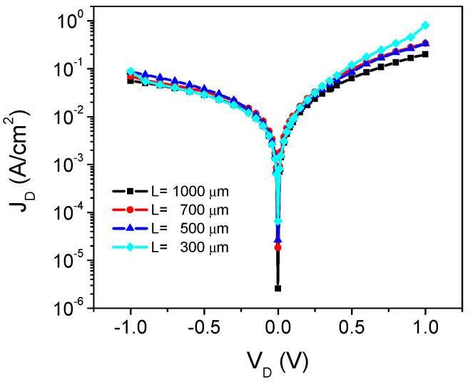
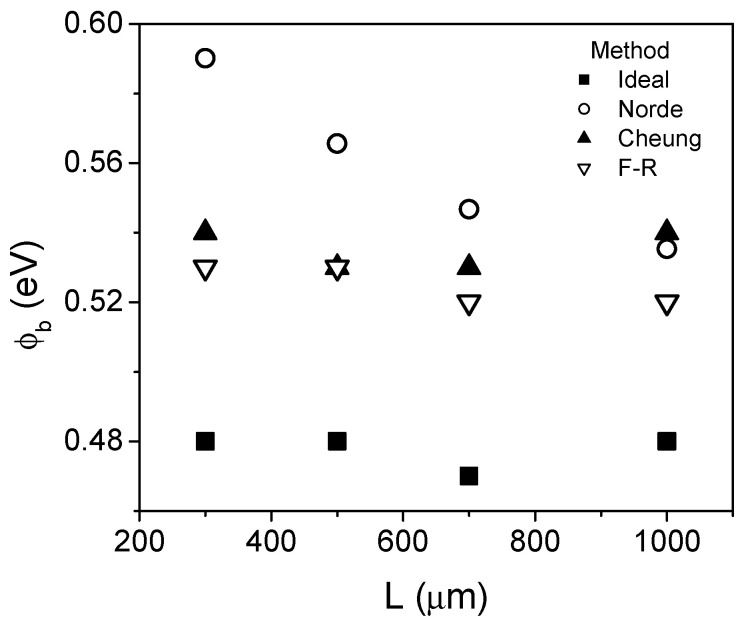
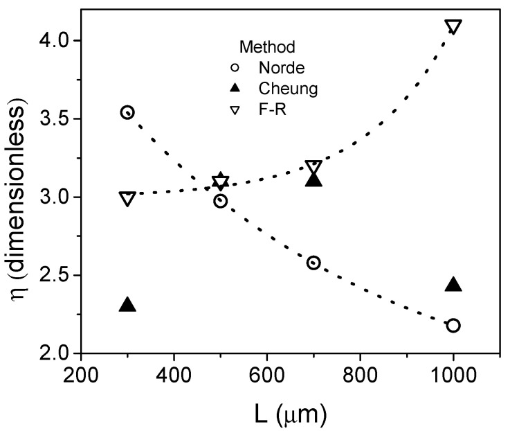
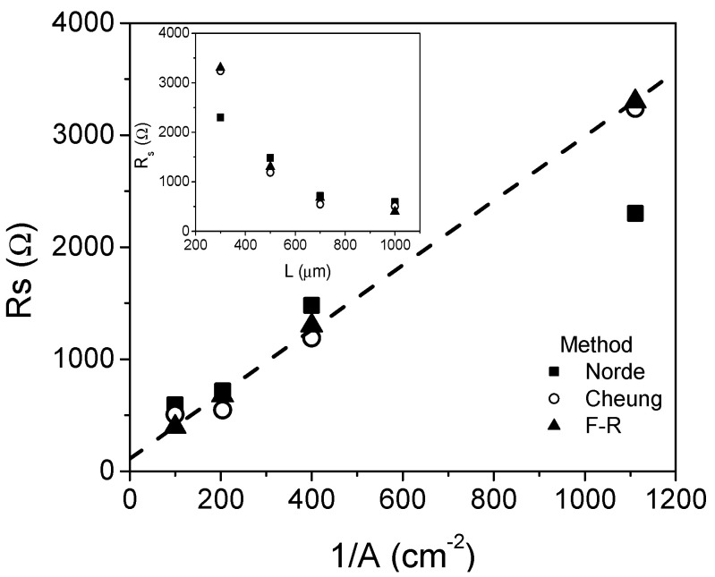
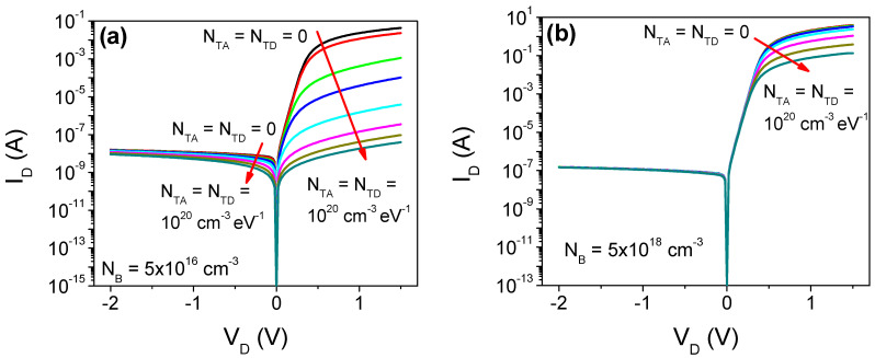
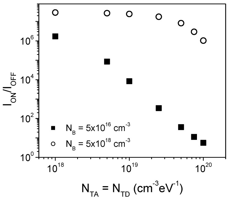
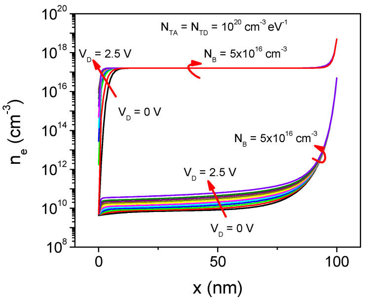
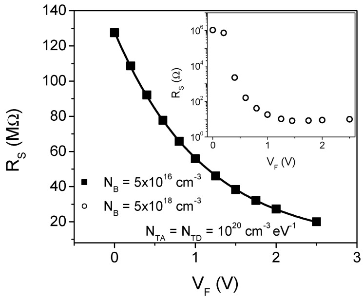
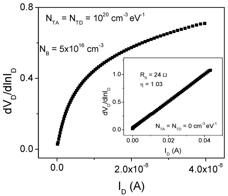
Schottky barrier diodes, developed by low-cost techniques and low temperature processes (LTP-SBD), have gained attention for different kinds of novel applications, including flexible electronic fabrication. This work analyzes the behavior of the I-V characteristic of solution processed, ZnO Schottky barrier diodes, fabricated at a low temperature. It is shown that the use of standard extraction methods to determine diode parameters in these devices produce significant dispersion of the ideality factor with values from 2.2 to 4.1, as well as a dependence on the diode area without physical meaning. The analysis of simulated I-V characteristic of LTP-SBD, and its comparison with experimental measurements, confirmed that it is necessary to consider the presence of a density of states (DOS) in the semiconductor gap, to understand specific changes observed in their performance, with respect to standard SBDs. These changes include increased values of Rs, as well as its dependence on bias, an important reduction of the diode current and small rectification values (RR). Additionally, it is shown that the standard extraction methodologies cannot be used to obtain diode parameters of LTP-SBD, as it is necessary to develop adequate parameter extraction methodologies for them.
Keywords: Schottky barrier diodes; semiconductor defects; solution-processing electronics; zinc oxide films.
Conflict of interest statement
The authors declare no conflict of interest.
Figures
References
-
- Baeg K.-J., Lee J. Flexible Electronic Systems on Plastic Substrates and Textiles for Smart Wearable Technologies. Adv. Mater. Technol. 2020;5:2000071. doi: 10.1002/admt.202000071. - DOI
-
- Berger P.R., Li M., Mattei R.M., Niang M.A., Talisa N., Tripepi M., Harris B., Bhalerao S.R., Chowdhury E.A., Winter C.H., et al. Advancements in Solution Processable Devices using Metal Oxides For Printed Internet-of-Things Objects; Proceedings of the IEEE Electron Devices Technology and Manufacturing Conference (EDTM); Singapore. 12–15 March 2019; - DOI
-
- Chan K.-Y., Ng Z.-N., Au B.W.-C., Knipp D. Visibly transparent metal oxide diodes prepared by solution processing. Opt. Mater. 2018;75:595–600. doi: 10.1016/j.optmat.2017.10.047. - DOI
-
- Rouis A., Hizem N., Kalboussi A. Electrical characterizations of Schottky diode with zinc oxide nanowires; Proceedings of the IEEE International Conference on Design & Test of Integrated Micro & Nano-Systems (DTS); Gammarth, Tunisia. 28 April–1 May 2019; - DOI
-
- Ahmeda M.A.M., Mwankemwa B.S., Carleschi E., Doyle B.P., Meyer W.E., Nel J.M. Effect of Sm doping ZnO nanorods on structural optical and electrical properties of Schottky diodes prepared by chemical bath deposition. Mater. Sci. Semicond. Processing. 2018;79:53–60. doi: 10.1016/j.mssp.2018.02.003. - DOI
LinkOut - more resources
Full Text Sources
Miscellaneous
