. 2022 May 11;12(10):1640.
doi: 10.3390/nano12101640.

The Graphene Structure's Effects on the Current-Voltage and Photovoltaic Characteristics of Directly Synthesized Graphene/n-Si(100) Diodes

Affiliations

The Graphene Structure's Effects on the Current-Voltage and Photovoltaic Characteristics of Directly Synthesized Graphene/n-Si(100) Diodes

Šarūnas Jankauskas et al. Nanomaterials (Basel). .

Abstract

Graphene was synthesized directly on Si(100) substrates by microwave plasma-enhanced chemical vapor deposition (MW-PECVD). The effects of the graphene structure on the electrical and photovoltaic properties of graphene/n-Si(100) were studied. The samples were investigated using Raman spectroscopy, atomic force microscopy, and by measuring current-voltage (I-V) graphs. The temperature of the hydrogen plasma annealing prior to graphene synthesis was an essential parameter regarding the graphene/Si contact I-V characteristics and photovoltaic parameters. Graphene n-type self-doping was found to occur due to the native SiO2 interlayer at the graphene/Si junction. It was the prevalent cause of the significant decrease in the reverse current and short-circuit current. No photovoltaic effect dependence on the graphene roughness and work function could be observed.

Keywords: MW-PECVD; graphene; photovoltaics.


Conflict of interest statement

The authors declare no conflict of interest.

Figures

Figure 1
Figure 1
Schematic diagram of the graphene/n-Si(100) fabricated diodes.
Figure 2
Figure 2
Typical Raman scattering spectra (a) and typical I−V characteristics (b) of directly synthesized graphene/Si(100) devices. The I−V characteristics of the device produced from the C2 sample exhibited diode behavior (red), ohmic contact was seen for the device produced from a sample B3 (green), and the A1 sample had diode-like I-V features (blue).
Figure 3
Figure 3
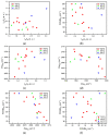
Relation between different Raman scattering spectra parameters: (a) I2D/IG vs. ID/IG; (b) FWHM2D vs. I2D/IG; (c) Pos2D vs. I2D/IG; (d) Pos2D vs. PosG; (e) FWHM2D vs. Pos2D; (f) FWHM2D vs. FWHMG. Samples were grouped according to the temperature of Si(100) substrate hydrogen plasma annealing before graphene growth: 700 °C (red), 800 °C (green), 900 °C (blue).
Figure 4
Figure 4
I−V characteristic parameters (IR(0.3 V), IR(0.1 V)/IF(0.1 V), IR(0.3 V)/IF(0.3 V)) in relation with: (ac) FWHMG; (df) Pos2D; and (gi) FWHM2D. Samples were grouped according to the temperature of Si(100) substrate hydrogen plasma annealing before graphene growth: 700 °C (red), 800 °C (green), 900 °C (blue).
Figure 5
Figure 5
Typical I−V characteristics of directly synthesized graphene/Si heterojunctions measured under the illumination by 800 nm wavelength (solid) and 406 nm wavelength (dashed) LEDs.
Figure 6
Figure 6
Structural effects on graphene/Si(100) diode’s photovoltaic parameters at 800 nm illumination: (a) ISC vs. I2D/IG plot; (b) UOC and I2D/IG relation; (c) ISC relation with FWHM2D; (d) UOC vs. FWHM2D plot; (e) ISC with respect to Raman 2D peak position; and (f) ISC and PosG correlation. Samples were grouped according to the temperature of Si(100) substrate hydrogen plasma annealing before graphene growth: 700 °C (red), 800 °C (green), 900 °C (blue).
Figure 7
Figure 7
Diode I−V and photovoltaic parameter (at 800 nm illumination) relation: (a) ISC vs. IR(0.3 V) plot; ISC correlation with diode’s I-V curve shape estimated using reverse and forward current ratio measured at 0.1 V (b) and 0.3 V (c); UOC vs. ISC/IR(0.3 V) plot (d) (solid and hollow markers indicate device illumination at 800 and 406 nm, respectively).

References

    1. Novoselov K.S. Electric Field Effect in Atomically Thin Carbon Films. Science. 2004;306:666–669. doi: 10.1126/science.1102896. - DOI - PubMed
    1. Nair R.R., Blake P., Grigorenko A.N., Novoselov K.S., Booth T.J., Stauber T., Peres N.M.R., Geim A.K. Fine Structure Constant Defines Visual Transparency of Graphene. Science. 2008;320:1308. doi: 10.1126/science.1156965. - DOI - PubMed
    1. Morozov S.V., Novoselov K.S., Katsnelson M.I., Schedin F., Elias D.C., Jaszczak J.A., Geim A.K. Giant Intrinsic Carrier Mobilities in Graphene and Its Bilayer. Phys. Rev. Lett. 2008;100:016602. doi: 10.1103/PhysRevLett.100.016602. - DOI - PubMed
    1. Lee C., Wei X., Kysar J.W., Hone J. Measurement of the Elastic Properties and Intrinsic Strength of Monolayer Graphene. Science. 2008;321:385–388. doi: 10.1126/science.1157996. - DOI - PubMed
    1. Bonaccorso F., Sun Z., Hasan T., Ferrari A.C. Graphene Photonics and Optoelectronics. Nat. Photonics. 2010;4:611–622. doi: 10.1038/nphoton.2010.186. - DOI

LinkOut - more resources