. 2022 May 17;12(10):1714.
doi: 10.3390/nano12101714.

Study of Electronic and Transport Properties in Double-Barrier Resonant Tunneling Systems

Affiliations

Study of Electronic and Transport Properties in Double-Barrier Resonant Tunneling Systems

John A Gil-Corrales et al. Nanomaterials (Basel). .

Abstract

Resonant tunneling devices are still under study today due to their multiple applications in optoelectronics or logic circuits. In this work, we review an out-of-equilibrium GaAs/AlGaAs double-barrier resonant tunneling diode system, including the effect of donor density and external potentials in a self-consistent way. The calculation method uses the finite-element approach and the Landauer formalism. Quasi-stationary states, transmission probability, current density, cut-off frequency, and conductance are discussed considering variations in the donor density and the width of the central well. For all arrangements, the appearance of negative differential resistance (NDR) is evident, which is a fundamental characteristic of practical applications in devices. Finally, a comparison of the simulation with an experimental double-barrier system based on InGaAs with AlAs barriers reported in the literature has been obtained, evidencing the position and magnitude of the resonance peak in the current correctly.

Keywords: Landauer formalism; electronic transmission probability; resonant tunneling diode.


Conflict of interest statement

The authors declare no conflict of interest.

Figures

Figure 1
Figure 1
Scheme of the resonant tunneling diode (RTD), with doping nd in the outer regions, two Al0.3Ga0.7As barriers, a GaAs well, and two outer regions of the GaAs undoped with two metal contacts in the external regions.
Figure 2
Figure 2
Conduction band profile. The dashed line correspond to the quasi-Fermi Level. The calculations are for Lw=4 nm, Lb=3 nm, Ls=3 nm, Ld=12 nm and nd=1.2×1018 cm3.
Figure 3
Figure 3
Potential energy for the system in equilibrium (bias voltage 0.0 V), the blue curve corresponds to the probability density of the resonant state, and the red dashed curve is the energy for this state E0. The quasi-Fermi level is also presented with the blue dashed curve. The calculations are for Lw=4 nm, Lb=3 nm, Ls=3 nm, Ld=12 nm and nd=1.2×1018 cm3.
Figure 4
Figure 4
Potential energy change with bias voltage from 0.0 V to 0.4 V, the blue curve corresponds to the resonant state probability density and the red curve is the energy for this state E0. The quasi-Fermi level is also presented by the dark blue dashed line for emitter and collector. The calculations are for Lw=4 nm, Lb=3 nm, Ls=3 nm, Ld=12 nm, and nd=1.2×1018 cm3.
Figure 5
Figure 5
Transmission coefficient for different values of bias voltage, the black curve is for Lw = 4 nm and, the red curve is for Lw = 10 nm. (a) with nd fixed at 1.2×10¹⁸ [1/cm3] and (b) with nd fixed at 10×1018 [1/cm3]. The shaded area indicates the region between the bottom of the conduction band and the quasi-Fermi level at the emitter. As indicated by the arrow in (b), the voltage for each curve varies from 0.0 V to 0.6 V in steps of 0.05 V.
Figure 6
Figure 6
Transmission coefficient for different values of Lw, the red curve corresponds to 0.0 V, and the black curve corresponds to 0.4 V. (a) with nd fixed at 1.2×10¹⁸ [1/cm3], and (b) with nd fixed at 10×1018 [1/cm3]. The shaded area indicates the region between the bottom of the conduction band and the quasi-Fermi level at the emitter.
Figure 7
Figure 7
Tunneling current density for two different values of Lw as a function of bias voltage, in (a) with nd = 1.2×10¹⁸ [1/cm3], and (b) with nd = 10×1018 [1/cm3]. Figure (c) shows the transmission for three different values of the Al concentration in the barriers, x = 0.2, 0.3, and 0.4 for a system of three regions AlxGa1xAs/GaAs/AlxGa1xAs. The inset shows the current density for these three systems taking Lw = 4 nm and Lb = 3 nm. In figures (a,b), the cut-off frequencies have been included for all the arrangements calculated (black text corresponds to Lw = 4 nm and red text corresponds to Lw = 10 nm) by taking two different values of τ0, 0.1 ps and 0.2 ps.
Figure 8
Figure 8
(a) Conductance for Lw=4 nm, for two different donor concentrations in units of G0=e2/π2, solid black line nd = 1.2×10¹⁸ [1/cm3], and dashed red line nd = 10×1018 [1/cm3]. (b) Corresponding self-consistent potentials. The curves were calculated at T=5 K.
Figure 9
Figure 9
(a) Conductance for Lw=10 nm, for two different donor concentrations in units of G0=e2/π2, solid black line nd = 1.2×10¹⁸ [1/cm3], and dashed red line nd = 10×1018 [1/cm3]. (b) Corresponding self-consistent potentials. The curves were calculated at T=5 K.
Figure 10
Figure 10
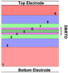
RTD structure composed of 9 layers that are expanded in detail in Table 3. DBRTD stands for Double-Barrier Resonant Tunneling Diode.
Figure 11
Figure 11
Self-consistent potential corresponding to the conduction band obtained numerically with the experimental parameters detailed in Table 3.
Figure 12
Figure 12
Comparison between simulated results using Equation (13) (red and blue dots) and experimental results [54] (black stars).

References

    1. Brown E.R., Söderström J.R., Parker C.D., Mahoney L.J., Molvar K.M., McGill T.C. Oscillations up to 712 GHz in InAs/AlSb resonant-tunneling diodes. Appl. Phys. Lett. 1991;58:2291–2293. doi: 10.1063/1.104902. - DOI
    1. Miyamoto T., Yamaguchi A., Mukai T. Terahertz imaging system with resonant tunneling diodes. Jpn. J. Appl. Phys. 2016;55:032201. doi: 10.7567/JJAP.55.032201. - DOI
    1. Bezhko M., Suzuki S., Asada M. Frequency increase in resonant-tunneling diode cavity-type terahertz oscillator by simulation-based structure optimization. Jpn. J. Appl. Phys. 2020;59:032004. doi: 10.35848/1347-4065/ab7355. - DOI
    1. Yachmeneva A.E., Pushkareva S.S., Reznikb R.R., Khabibullina R.A., Ponomarev D.S. Arsenides-and related III-V materials-based multilayered structures for terahertz applications: Various designs and growth technology. Prog. Cryst. Growth Charact. Mater. 2020;66:100485. doi: 10.1016/j.pcrysgrow.2020.100485. - DOI
    1. Andrews A.M., Korb H.W., Holonyak N., Duke C.B., Kleiman G.G. Tunnel mechanisms and junction characterization in III-V tunnel diodes. Phys. Rev. B. 1972;5:2273–2295. doi: 10.1103/PhysRevB.5.2273. - DOI

LinkOut - more resources