. 2022 Jun 6;13(1):3255.
doi: 10.1038/s41467-022-30983-4.

Ferroelectric domain-wall logic units

Affiliations

Ferroelectric domain-wall logic units

Jing Wang et al. Nat Commun. .

Abstract

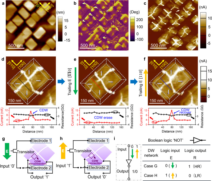
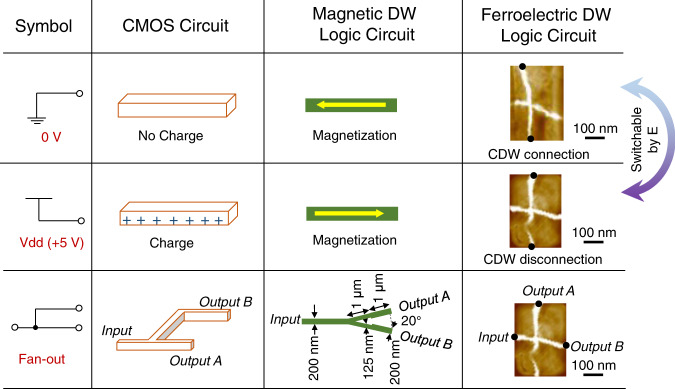
The electronic conductivities of ferroelectric domain walls have been extensively explored over the past decade for potential nanoelectronic applications. However, the realization of logic devices based on ferroelectric domain walls requires reliable and flexible control of the domain-wall configuration and conduction path. Here, we demonstrate electric-field-controlled stable and repeatable on-and-off switching of conductive domain walls within topologically confined vertex domains naturally formed in self-assembled ferroelectric nano-islands. Using a combination of piezoresponse force microscopy, conductive atomic force microscopy, and phase-field simulations, we show that on-off switching is accomplished through reversible transformations between charged and neutral domain walls via electric-field-controlled domain-wall reconfiguration. By analogy to logic processing, we propose programmable logic gates (such as NOT, OR, AND and their derivatives) and logic circuits (such as fan-out) based on reconfigurable conductive domain walls. Our work might provide a potentially viable platform for programmable all-electric logic based on a ferroelectric domain-wall network with low energy consumption.


Conflict of interest statement

The authors declare no competing interests.

Figures

Fig. 1
Fig. 1. Electric field control of the on-and-off switching of a CDW and a NOT gate.
a Morphology, b in-plane PFM phase, and (c) c-AFM image of vertex domains confined in a rectangular BiFeO3 nano-island array. d Initial cross-shaped CDW network with center-divergent (marked by three-dimensional arrows) vertex domains confined in a rectangular BiFeO3 nano-island. e Disconnection of a CDW branch by a [1¯1¯0]-oriented (marked by the green arrow) trailing field. f Reconnection of this disrupted CDW branch by a [110]-oriented (marked by yellow arrow) trailing field. The curves below panels (df) are the corresponding current profiles along the dashed lines in (df). g, h Schematic of two logic operations of the NOT gate based on the experimental observations in (e, f), where [1¯1¯0]- and [110]-oriented electric fields are defined as logic inputs ‘0’ and ‘1’, and the corresponding high and low resistance (HR and LR) states for the disconnected and connected CDW are defined as logic outputs ‘1’ and ‘0’, respectively. i Corresponding symbol (left) and truth table (right) for the NOT logic gate.
Fig. 2
Fig. 2. Mechanism of the tunability of CDWs by an electric field based on phase-field simulations.
a Polar vector map for a 178 × 138 nm2 nano-island with cross-shaped CDWs. b, c Polar vector maps for the rectangular nano-island after a [1¯1¯0]- or [110]-oriented electric field is applied in the area enclosed by the blue dotted box in (a). df Magnified polar vector maps for the area highlighted by the blue dotted boxes in (a, b, c), which show that the local DW is reversibly modulated between a CDW and a neutral DW by the local electric field. gi Corresponding charge density maps for (a, b, c). The connected CDWs in (g) and (i) and disconnected CDWs in (h) indicate a high conductance for the CDW and a low conductance for the neutral DW, respectively.
Fig. 3
Fig. 3. Reconfigurable NOR logic gate.
ad c-AFM images and corresponding logic circuit diagrams of two parallel-connected nano-islands with the sequence of logic operations for inputs of ‘11’, ‘10’, ‘01’, and ‘00’. e Truth table for the NOR logic gate. E1 and E2 are the applied in-plane trailing fields for the two nano-islands.
Fig. 4
Fig. 4. Reconfigurable OR logic gate.
ac CDW networks at the initial state and controlled by an in-plane trailing field in a BiFeO3 nano-island with an AR of 1.25. The connection/disconnection of A/B node and disconnection/connection of C/D node is implemented concurrently in one nano-island by applying an in-plane field along [1¯1¯0] (b) or [110] direction (c). dg c-AFM images and corresponding logic circuit diagrams of two series-connected nano-islands with the sequence of logic operations for inputs of ‘11’, ‘10’, ‘01’, and ‘00’. h Truth table for OR logic gate respectively. E1 and E2 are the applied  in-plane trailing fields for the two nano-islands. R represents the resistance of the DW between the output electrodes.
Fig. 5
Fig. 5. Electric field control of ferroelectric CDW logic circuits.
Schematic illustration of the ferroelectric DW logic circuits for the readout signal of low and high voltages and the fan-out function. The bidirectional arrow indicates that the readout signals of low and high voltages can be transformed into each other by electric-field-induced connection and disconnection of a CDW. The schematics for the CMOS circuit and magnetic DW logic circuit, redrawn from ref. are also illustrated for comparison. E represents the applied in-plane electric field.

References

    1. Catalan G, Seidel J, Ramesh R, Scott JF. Domain wall nanoelectronics. Rev. Mod. Phys. 2012;84:119–156. doi: 10.1103/RevModPhys.84.119. - DOI
    1. Meier D, Selbach SM. Ferroelectric domain walls for nanotechnology. Nat. Rev. Mater. 2022;7:157–173. doi: 10.1038/s41578-021-00375-z. - DOI
    1. Yang S-H, Naaman R, Paltiel Y, Parkin SSP. Chiral spintronics. Nat. Rev. Phys. 2021;3:328–343. doi: 10.1038/s42254-021-00302-9. - DOI
    1. Raymenants E, et al. Nanoscale domain wall devices with magnetic tunnel junction read and write. Nat. Electron. 2021;4:392–398. doi: 10.1038/s41928-021-00593-x. - DOI
    1. Li R, et al. A spin–orbit torque device for sensing three-dimensional magnetic fields. Nat. Electron. 2021;4:179–184. doi: 10.1038/s41928-021-00542-8. - DOI