Review
. 2022 May 20:10:905404.
doi: 10.3389/fchem.2022.905404. eCollection 2022.

2D Materials for Efficient Photodetection: Overview, Mechanisms, Performance and UV-IR Range Applications

Affiliations
Review

2D Materials for Efficient Photodetection: Overview, Mechanisms, Performance and UV-IR Range Applications

Maria Malik et al. Front Chem. .

Abstract

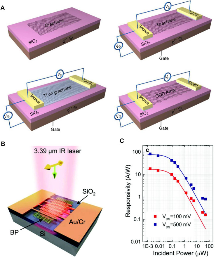
Two-dimensional (2D) materials have been widely used in photodetectors owing to their diverse advantages in device fabrication and manipulation, such as integration flexibility, availability of optical operation through an ultrabroad wavelength band, fulfilling of photonic demands at low cost, and applicability in photodetection with high-performance. Recently, transition metal dichalcogenides (TMDCs), black phosphorus (BP), III-V materials, heterostructure materials, and graphene have emerged at the forefront as intriguing basics for optoelectronic applications in the field of photodetection. The versatility of photonic systems composed of these materials enables their wide range of applications, including facilitation of chemical reactions, speeding-up of responses, and ultrasensitive light detection in the ultraviolet (UV), visible, mid-infrared (MIR), and far-infrared (FIR) ranges. This review provides an overview, evaluation, recent advancements as well as a description of the innovations of the past few years for state-of-the-art photodetectors based on two-dimensional materials in the wavelength range from UV to IR, and on the combinations of different two-dimensional crystals with other nanomaterials that are appealing for a variety of photonic applications. The device setup, materials synthesis, operating methods, and performance metrics for currently utilized photodetectors, along with device performance enhancement factors, are summarized.

Keywords: 2D materials; TMDC; UV-IR photodetectors; black phosphorus; graphene; heterostructures; mechanisms; performance factors.


Conflict of interest statement

The authors declare that the research was conducted in the absence of any commercial or financial relationships that could be construed as a potential conflict of interest.

Figures

FIGURE 1
FIGURE 1
Performance comparison of various 2D materials-based photodetectors, (A) Photoresponsivity of conventional materials and their heterostructures for IR photodetection, (B) Detectivity of 2D materials and their heterostructures for IR photodetection, and (C) Electromagnetic spectrum along with targeted ranges as summarized in this study.
FIGURE 2
FIGURE 2
A schematic representation of photodetection mechanisms, (A) Photovoltaic effect (Qiu and Huang, 2021), (B) Photo-thermoelectric effect (Qiu and Huang, 2021), (C) Bolometric effect (Qiu and Huang, 2021), and (D) Plasma wave assisted mechanism (Qiu and Huang, 2021); Reproduced with permission from (Qiu and Huang, 2021).
FIGURE 3
FIGURE 3
Photodetection mechanisms, (A,B) Schematic of photoconductive effect (Long et al., 2019), and (C) Schematic of photogating effect (Long et al., 2019); Reproduced with permission from (Long et al., 2019).
FIGURE 4
FIGURE 4
(A) Graphene structure (Roberts et al., 2010), and (B) Single layered atomic structure of TMDCs in trigonal prismatic (2H) distorted octahedral (1T) and dimerized (1T’) states (Manzeli et al., 2017). Adapted with permission from (Roberts et al., 2010; Manzeli et al., 2017).
FIGURE 5
FIGURE 5
(A) Multilayered crystal structure of black phosphorus (Shao et al., 2014), (B) Top view (Shao et al., 2014), and (C) Side view (Shao et al., 2014); Adapted with permission from (Shao et al., 2014).
FIGURE 6
FIGURE 6
Schematic of 2D material synthesis methodologies (A) Mechanical exfoliation technique (Huang et al., 2015), (B) Liquid phase exfoliation (Guo et al., 2015), and (C) Chemical vapor deposition (Cui et al., 2017); Reproduced with permission from (Guo et al., 2015; Huang et al., 2015; Cui et al., 2017).
FIGURE 7
FIGURE 7
(A) Graphene bi-layer bolometric device structure (Koppens et al., 2014), (B) Graphene–Al tunnel junction bolometer device structure (Koppens et al., 2014), (C) Photodetectors based on QDs (Konstantatos et al., 2012), and (D) Resistance–voltage relationship for the graphene–QD structure (Konstantatos et al., 2012); Reproduced with permission from (Konstantatos et al., 2012; Koppens et al., 2014).
FIGURE 8
FIGURE 8
(A) Schematic of MoS2 single-layered phototransistor (George et al., 2021), and (B) Schematic of ReS2 photodetector (Liu et al., 2016a); Reproduced with permission from (Liu et al., 2016a; George et al., 2021).
FIGURE 9
FIGURE 9
(A) Schematic of MoS2 based photodetectors (Lopez-Sanchez et al., 2013), and (B) Schematic of WS2 based photodetectors (Koppens et al., 2014); Reproduced with permission from (Lopez-Sanchez et al., 2013; Koppens et al., 2014).
FIGURE 10
FIGURE 10
(A) Schematic of black phosphorus-based photodetector (Yan Liu et al., 2018), (B) BP photodetector responsivity (Yan Liu et al., 2018), (C) Schematic of BP-MoS2 photodetector (Ye et al., 2016b), and (D) BP-MoS2 photodetector responsivity (Ye et al., 2016b); Reproduced with permission from (Ye et al., 2016b; Yan Liu et al., 2018).
FIGURE 11
FIGURE 11
Schematic of (A) MoTe2/graphene-based photodetector (Kharadi et al., 2021), (B) Silicene/MoS2 based photodetectors (Kharadi et al., 2021), (C) (MSB)/WeS2 based photodetectors (Qiu and Huang, 2021), and (D) BP- WSe2 photodetector (Zong et al., 2020); Reproduced with permission from (Kharadi et al., 2021; Zong et al., 2020; Qiu and Huang, 2021).
FIGURE 12
FIGURE 12
2D heterostructure photodetectors (A,B) Schematic and responsivity spectra of hybrid graphene/Ti2O3 photodetector (Yu et al., 2018a), (C,D) PbI2 based photodetector and its photo-response spectra (Zhang et al., 2018), (E,F) Graphene-MoS2 photodetector and its photoresponsivity (Deng et al., 2018b), (G,H) Schematic of PtTe2 based photodetector and its responsivity spectra (Xu et al., 2019); Reproduced with permission from (Yu et al., 2018a; Deng et al., 2018b; Zhang et al., 2018; Xu et al., 2019).
FIGURE 13
FIGURE 13
(A) Schematic of graphene-QD-based photodetector (Zhang et al., 2015), (B) Time response of graphene-QD-based photodetector (Zhang et al., 2015); Reproduced with permission from (Zhang et al., 2015).
FIGURE 14
FIGURE 14
(A) Photoresponsivity of BP based photodetector (Wu et al., 2015), (B) Photoresponsivity of MoS2-NCs based photodetector (Alkis et al., 2012), (C) Photoresponsivity and detectivity of WS2 based photodetector (Zeng et al., 2016), (D) Optical image of GaS thin film-based photodetector (Hu et al., 2013), and (E) Responsivity and photo-detectivity of GaS thin film-based photodetector (Hu et al., 2013); Reproduced with permission from (Hu et al., 2013; Wu et al., 2015; Alkis et al., 2012; Zeng et al., 2016).
FIGURE 15
FIGURE 15
(A) Graphene photodetector with different metal contacts (Mueller et al., 2010), (B) Schematic of graphene stacked device (Chen et al., 2015), (C) Graphene stacked based photon energy dependence on IQE, (D) Monolayered MoSe2 photodetector (Wang et al., 2018), (E) With its time resolved current (Wang et al., 2018), (F) Multilayered RSe2 photodetector (Liu et al., 2016b), and (G) With its responsivity (Liu et al., 2016b); Reproduced with permission from (Mueller et al., 2010; Liu et al., 2016b; Chen et al., 2015; Wang et al., 2018).
FIGURE 16
FIGURE 16
(A) schematic of BP based photodetector (Buscema et al., 2014), (B) schematic of BP-MoS2 based photodetector (Deng et al., 2014), (C) BP-MoS2 based photodetector responsivity, (D) schematic of InSe based photodetector (Wu et al., 2016), (E) schematic of GaSe-GaSb based heterostructure photodetector (Wang et al., 2017), and (F) GaSe-GaSb based heterostructure photodetector responsivity (Wang et al., 2017); Reproduced with permission from (Buscema et al., 2014; Deng et al., 2014; Wu et al., 2016; Wang et al., 2017).
FIGURE 17
FIGURE 17
(A) Fabrication process of graphene-based photodetector band engineering (Zhang et al., 2013b), (B) Schematic of BP based photodetectors, and (C) BP based photodetector responsivity (Guo et al., 2016); Reproduced with permission from (Zhang et al., 2013b; Guo et al., 2016).
FIGURE 18
FIGURE 18
2D materials-based photodetector processes, perspectives, challenges, and applications.

Similar articles

Cited by

References

    1. Abderrahmane A., Ko P. J., Thu T. V., Ishizawa S., Takamura T., Sandhu A. (2014). High Photosensitivity Few-Layered MoSe2 Back-Gated Field-Effect Phototransistors. Nanotechnology 25 (36), 365202. 10.1088/0957-4484/25/36/365202 - DOI - PubMed
    1. Adhikari K. R. (2017). Thermocouple: Facts and Theories. Himal. Phys. 2017, 10–14. 10.3126/hj.v6i0.18350 - DOI
    1. Ahn J., Ko K., Kyhm J.-h., Ra H.-S., Bae H., Hong S., et al. (2021). Near-Infrared Self-Powered Linearly Polarized Photodetection and Digital Incoherent Holography Using WSe2/ReSe2 van der Waals Heterostructure. ACS Nano 15 (11), 17917–17925. 10.1021/acsnano.1c06234 - DOI - PubMed
    1. Akinwande D., Huyghebaert C., Wang C.-H., Serna M. I., Goossens S., Li L.-J., et al. (2019). Graphene and Two-Dimensional Materials for Silicon Technology. Nature 573 (7775), 507–518. 10.1038/s41586-019-1573-9 - DOI - PubMed
    1. Alkis S., Öztaş T., Aygün L. E., Bozkurt F., Okyay A. K., Ortaç B. (2012). Thin Film MoS2 Nanocrystal Đ Based Ultraviolet Photodetector. Opt. Express 20 (19), 21815–21820.Ñ2. 10.1364/oe.20.021815 - DOI - PubMed