Multilevel polarization switching in ferroelectric thin films
- PMID: 35672404
- PMCID: PMC9174202
- DOI: 10.1038/s41467-022-30823-5
Multilevel polarization switching in ferroelectric thin films
Abstract
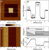
Ferroic order is characterized by hystereses with two remanent states and therefore inherently binary. The increasing interest in materials showing non-discrete responses, however, calls for a paradigm shift towards continuously tunable remanent ferroic states. Device integration for oxide nanoelectronics furthermore requires this tunability at the nanoscale. Here we demonstrate that we can arbitrarily set the remanent ferroelectric polarization at nanometric dimensions. We accomplish this in ultrathin epitaxial PbZr0.52Ti0.48O3 films featuring a dense pattern of decoupled nanometric 180° domains with a broad coercive-field distribution. This multilevel switching is achieved by driving the system towards the instability at the morphotropic phase boundary. The phase competition near this boundary in combination with epitaxial strain increases the responsiveness to external stimuli and unlocks new degrees of freedom to nano-control the polarization. We highlight the technological benefits of non-binary switching by demonstrating a quasi-continuous tunability of the non-linear optical response and of tunnel electroresistance.
© 2022. The Author(s).
Conflict of interest statement
The authors declare no competing interests.
Figures


Similar articles
-
Tunneling electroresistance in multiferroic heterostructures.Nanotechnology. 2014 Dec 12;25(49):495203. doi: 10.1088/0957-4484/25/49/495203. Epub 2014 Nov 21. Nanotechnology. 2014. PMID: 25414163
-
Ferroelastic Nanodomain-mediated Mechanical Switching of Ferroelectricity in Thick Epitaxial Films.Nano Lett. 2021 Jan 13;21(1):445-452. doi: 10.1021/acs.nanolett.0c03875. Epub 2020 Dec 2. Nano Lett. 2021. PMID: 33264026
-
Rhombohedral-Orthorhombic Ferroelectric Morphotropic Phase Boundary Associated with a Polar Vortex in BiFeO3 Films.ACS Nano. 2018 Nov 27;12(11):11098-11105. doi: 10.1021/acsnano.8b05449. Epub 2018 Oct 25. ACS Nano. 2018. PMID: 30352155
-
In situmonitoring of epitaxial ferroelectric thin-film growth.J Phys Condens Matter. 2021 Jun 9;33(29). doi: 10.1088/1361-648X/abf979. J Phys Condens Matter. 2021. PMID: 33873174 Review.
-
Effects of Interfaces on the Structure and Novel Physical Properties in Epitaxial Multiferroic BiFeO₃ Ultrathin Films.Materials (Basel). 2014 Jul 23;7(7):5403-5426. doi: 10.3390/ma7075403. Materials (Basel). 2014. PMID: 28788135 Free PMC article. Review.
Cited by
-
Experimental demonstration of tunable hybrid improper ferroelectricity in double-perovskite superlattice films.Nat Commun. 2024 Jul 2;15(1):5549. doi: 10.1038/s41467-024-49707-x. Nat Commun. 2024. PMID: 38956065 Free PMC article.
-
Lead-Free Perovskite Thin Films with Tailored Pockels-Kerr Effects for Photonics.ACS Appl Mater Interfaces. 2023 Aug 9;15(31):38039-38048. doi: 10.1021/acsami.3c06499. Epub 2023 Jul 27. ACS Appl Mater Interfaces. 2023. PMID: 37497599 Free PMC article.
-
Reversible control over the distribution of chemical inhomogeneities in multiferroic BiFeO3.Nat Commun. 2025 Apr 27;16(1):3951. doi: 10.1038/s41467-025-59044-2. Nat Commun. 2025. PMID: 40289179 Free PMC article.
-
High-performance van der Waals antiferroelectric CuCrP2S6-based memristors.Nat Commun. 2023 Nov 30;14(1):7891. doi: 10.1038/s41467-023-43628-x. Nat Commun. 2023. PMID: 38036500 Free PMC article.
-
Proton-mediated reversible switching of metastable ferroelectric phases with low operation voltages.Sci Adv. 2023 May 24;9(21):eadg4561. doi: 10.1126/sciadv.adg4561. Epub 2023 May 24. Sci Adv. 2023. PMID: 37224248 Free PMC article.
References
-
- Kakekhani A, Ismail-Beigi S. Ferroelectric-based catalysis: Switchable surface chemistry. ACS Catal. 2015;5:4537–4545. doi: 10.1021/acscatal.5b00507. - DOI
-
- Markovic D, Mizrahi A, Querlioz D, Grollier J. Physics for neuromorphic computing. Nat. Rev. Phys. 2020;2:499–510. doi: 10.1038/s42254-020-0208-2. - DOI
Grants and funding
- CRSK-2_196061/Schweizerischer Nationalfonds zur Förderung der Wissenschaftlichen Forschung (Swiss National Science Foundation)
- 200021_175926/Schweizerischer Nationalfonds zur Förderung der Wissenschaftlichen Forschung (Swiss National Science Foundation)
- 200021_188414/Schweizerischer Nationalfonds zur Förderung der Wissenschaftlichen Forschung (Swiss National Science Foundation)
- CRSK-2_196061/Schweizerischer Nationalfonds zur Förderung der Wissenschaftlichen Forschung (Swiss National Science Foundation)
- 694955-INSEETO/EC | EU Framework Programme for Research and Innovation H2020 | H2020 Priority Excellent Science | H2020 European Research Council (H2020 Excellent Science - European Research Council)
- 694955-INSEETO/EC | EU Framework Programme for Research and Innovation H2020 | H2020 Priority Excellent Science | H2020 European Research Council (H2020 Excellent Science - European Research Council)
- 694955-INSEETO/EC | EU Framework Programme for Research and Innovation H2020 | H2020 Priority Excellent Science | H2020 European Research Council (H2020 Excellent Science - European Research Council)
LinkOut - more resources
Full Text Sources

