. 2022 Jun 14;13(1):3431.
doi: 10.1038/s41467-022-29976-0.

Beam steering at the nanosecond time scale with an atomically thin reflector

Affiliations

Beam steering at the nanosecond time scale with an atomically thin reflector

Trond I Andersen et al. Nat Commun. .

Abstract

Techniques to mold the flow of light on subwavelength scales enable fundamentally new optical systems and device applications. The realization of programmable, active optical systems with fast, tunable components is among the outstanding challenges in the field. Here, we experimentally demonstrate a few-pixel beam steering device based on electrostatic gate control of excitons in an atomically thin semiconductor with strong light-matter interactions. By combining the high reflectivity of a MoSe2 monolayer with a graphene split-gate geometry, we shape the wavefront phase profile to achieve continuously tunable beam deflection with a range of 10°, two-dimensional beam steering, and switching times down to 1.6 nanoseconds. Our approach opens the door for a new class of atomically thin optical systems, such as rapidly switchable beam arrays and quantum metasurfaces operating at their fundamental thickness limit.


Conflict of interest statement

Harvard University has filed a provisional patent application (No. 63/153,726) for a fast spatial light modulator based on an atomically thin reflector, with the following inventors: T.I.A., R.J.G., G.S., B.L.D., D.S.W., R.B., A.S., S.F.Y., P.K., H.P., and M.D.L.

Figures
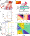
Fig. 1
Fig. 1. Continuously tunable phase patterning in a van der Waals heterostructure.
a Schematic of our approach: patterned electrostatic doping of atomically thin transition metal dichalcogenides (TMDs) allows for spatial control of the exciton resonance (inset). Thus, a continuously tunable phase profile is imparted on the reflected wavefront, enabling wide-ranging possibilities for beam control. b Schematic of SG-FET structure. Since the bottom gate only covers part of the device, the phase can be tuned independently in the two sides. The phase discontinuity in the reflected wavefront causes the two halves to constructively interfere at an angle in the far field. Inset: zoomed-in optical microscope image of the device, with gate edge indicated by white dashed line. c Representative reflection spectrum (orange) from left side of gate edge in intrinsic regime (VBG = 0 V and VTG = 0.5 V), with asymmetric resonance fit (black), which allows for extracting the phase (red). d, e Gate dependence of λleft and λright, respectively (locations indicated by circles in inset of b). The exciton resonance blue-shifts upon electrostatic doping. While λleft depends on 8VTG+ VBG, λright is largely independent of VBG. The intrinsic regime appears at an offset of VTG = 0.5 V, likely due to charge collection at the top gate. The small voltage range of the intrinsic regime suggests some doping via in-gap states. f Reflection spectra from left (orange) and right (blue) side of gate edge at different gate voltage combinations shown as correspondingly colored crosses in g. Dashed gray line indicates λ0 = 755.6 nm. g Gate dependence of phase difference Δϕ between the right and left side at λ0 = 755.6 nm, computed from fits as in (c). A tunable Δϕ-range of 42° is achieved. Large positive Δϕ is achieved when λleft < λ0 < λright (blue cross), while large negative Δϕ is achieved when λright < λ0 < λleft (green). Δϕ is closer to zero when either both sides are doped (λleft, λright < λ0; yellow) or both are intrinsic (λ0 < λleft, λright; red).
Fig. 2
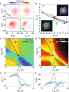
Fig. 2. Continuously tunable beam steering.
a Fourier images of reflected beam (λ0 = 755.6 nm) in the four regimes after subtracting the reflection in the highly doped regime (VBG = 10 V and VTG = 1.4 V). When the exciton resonance is blue-shifted past λ0 in only one side of the device (blue, green), the beam is deflected away from that side. If neither or both are blue-shifted past λ0, the phase difference is small and little deflection is observed (red, yellow). b Scatter plot of the beam deflection (θ¯x,θ¯y) for the full range of gate voltages, showing that the deflection is perpendicular to the gate edge (dashed line) and continuously tunable. Inset: Fourier images without background subtraction. c The gate dependence of the deflection perpendicular to the gate edge (θ¯) is in very good agreement with that of the phase difference shown in Fig. 1g. d Gate dependence of reflection amplitude. Regions with high reflection indicate that one of the resonances crosses through λ0. e, f Linecuts indicated by dashed black, teal, and gray lines in (c) and (d), respectively, highlighting the continuous steering capability and that the reflection can be kept relatively constant while deflecting the beam. Connecting lines in e and f are guides to the eye.
Fig. 3
Fig. 3. Two-dimensional beam steering.
a Zoomed-in optical image of device, indicating regions of monolayer and bilayer MoSe2, as well as gate coverage. By tuning the relative phase and amplitude of the reflection from the three regions, more intricate wavefront phase profiles can be achieved. b Reflection spectra from the dual-gated monolayer (black), single-gated monolayer (gray) and the bilayer (purple) in the intrinsic regime (VBG = 0 V and VTG = 0.5 V). Since the resonance is red-shifted in the bilayer, it acts as a dielectric (non-resonant) reflector at the wavelengths used here. c Fourier images of reflected beam (λ0 = 754.1 nm) in the four regimes after subtracting reflection in the highly doped regime (VBG = 10 V and VTG = 1.4 V). The beam is now steered in two dimensions. Red: when both monolayer resonances are red-shifted relative to λ0, their phase is higher than in the bilayer region, causing the beam to deflect upwards. Blue and green: when one of the monolayer resonances is kept red-shifted relative to λ0, the beam is deflected towards that monolayer region. d Scatter plot of the center-of-mass deflection (θ¯x,θ¯y), with the points from (c) highlighted. The set of beam deflections now span a two-dimensional area. e, f Gate dependence of θ¯x (e) and θ¯y (f). While the gate dependence resembles that of the phase in Fig. 1g, θ¯x and θ¯y are now less coupled. g Center-of-mass deflection tracing out “PHYSICS” (rotated 148° counter-clockwise) by applying a sequence of gate voltage combinations.
Fig. 4
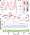
Fig. 4. High-frequency beam steering.
a Oscillations of center-of-mass deflection (λ0 = 754.5 nm) induced by oscillating back gate voltage (offset, V0 = 0.7 V; amplitude, ΔV = 0.45 V; period, τ =2 s) and VTG = 0.64 V. b, c Fourier plane images collected at VBG =V0 + ΔV (b) and VBG = V0 − ΔV (c), as indicated by circles in a, after subtracting reflection at VBG = V0. An inverted telescope was used to shrink the beam to simplify the subsequent APD measurements. d Photon count oscillations measured with APD at τ = 10 μs, 100 ns, 5.6 ns, and 3.2 ns (top to bottom). Darker (lighter) shade curves show photon counts from left (right) side of Fourier plane, as indicated by the inset in the top panel. All curves are normalized to the corresponding contrast at τ = 10 μs.

References

    1. Yu N, Capasso F. Flat optics with designer metasurfaces. Nat. Mater. 2014;13:139–150. doi: 10.1038/nmat3839. - DOI - PubMed
    1. Kildishev AV, Boltasseva A, Shalaev VM. Planar photonics with metasurfaces. Science. 2013;339:1232009. doi: 10.1126/science.1232009. - DOI - PubMed
    1. Lin D, Fan P, Hasman E, Brongersma ML. Dielectric gradient metasurface optical elements. Science. 2014;345:298–302. doi: 10.1126/science.1253213. - DOI - PubMed
    1. Khorasaninejad M, et al. Metalenses at visible wavelengths: diffraction-limited focusing and subwavelength resolution imaging. Science. 2016;352:1190–1194. doi: 10.1126/science.aaf6644. - DOI - PubMed
    1. Wang Z, et al. Exciton-enabled meta-optics in two-dimensional transition metal dichalcogenides. Nano Lett. 2020;20:7964–7972. doi: 10.1021/acs.nanolett.0c02712. - DOI - PubMed