Review
. 2022 Jul 1;12(13):2260.
doi: 10.3390/nano12132260.

Mid-Infrared Optoelectronic Devices Based on Two-Dimensional Materials beyond Graphene: Status and Trends

Affiliations
Review

Mid-Infrared Optoelectronic Devices Based on Two-Dimensional Materials beyond Graphene: Status and Trends

Rui Cao et al. Nanomaterials (Basel). .

Abstract

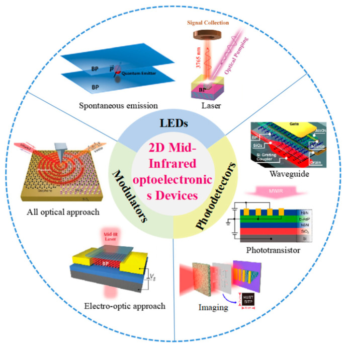
Since atomically thin two-dimensional (2D) graphene was successfully synthesized in 2004, it has garnered considerable interest due to its advanced properties. However, the weak optical absorption and zero bandgap strictly limit its further development in optoelectronic applications. In this regard, other 2D materials, including black phosphorus (BP), transition metal dichalcogenides (TMDCs), 2D Te nanoflakes, and so forth, possess advantage properties, such as tunable bandgap, high carrier mobility, ultra-broadband optical absorption, and response, enable 2D materials to hold great potential for next-generation optoelectronic devices, in particular, mid-infrared (MIR) band, which has attracted much attention due to its intensive applications, such as target acquisition, remote sensing, optical communication, and night vision. Motivated by this, this article will focus on the recent progress of semiconducting 2D materials in MIR optoelectronic devices that present a suitable category of 2D materials for light emission devices, modulators, and photodetectors in the MIR band. The challenges encountered and prospects are summarized at the end. We believe that milestone investigations of 2D materials beyond graphene-based MIR optoelectronic devices will emerge soon, and their positive contribution to the nano device commercialization is highly expected.

Keywords: mid-infrared; modulator; photodetectors; two-dimensional materials.


Conflict of interest statement

The authors declare no conflict of interest.

Figures

Figure 1
Figure 1
The 2D materials for various MIR optoelectronic applications.
Figure 2
Figure 2
(a) Normalized PL spectra of BP from 1 to 5 layers. (b) PL peak energy of different layers [185]. Copyright 2015 Nature Publishing Group. (c) Relationship between peak intensity and number of layers [186]. Copyright 2014 American Chemical Society. (d) Single layer BP diagram coupled with quantum emitter. (e) Double-layer BP diagram coupled with quantum emitter [187]. Copyright 2017 The Optical Society. (f) Embedded DBR microcavity embedded with BP nanosheets. (g) The cross-section view of microcavity embedded with BP inSEM image. (h) BP crystalline structure. (i) DBR and the SiO cavity transmission spectrum caught in the bottom and up DBRs. (fi) Reproduced with permission from Ref. [188]. Copyright 2020 Wiley-Blackwell.
Figure 3
Figure 3
(a) Power/current curve and emission spectra of ZnSe laser diodes with Te-terminated GaAs interface (inset). (b) As the electric field changes, the Te-started laser diode is displayed [189]. Copyright 1998 Elsevier. (c) Etching TeO2 waveguide and Er-doped waveguide. (d) Life time variation of erbium-doped acetate film [190]. Copyright 2010 The Optical Society. (e) The photoluminescence of Te solid crystals in the medium wavelength infrared (MWIR) region. (f) Temperature variation curve of MWIR emission spectrum of Te bulk crystal, and the curve of Te bulk crystal MWIR emission spectrum with laser intensity [197]. Copyright 2019 American Chemical Society.
Figure 4
Figure 4
(a) Pulse series and monopulse waveform (inset) are 489.3 mW and (b) 2.99 W, respectively, at the power of the transmitting pump. (c) The measured spectrum of the pulse. (d) The RF spectrum of the pulse. (e) Change curve of launched pump power with repetition rate. (f) Launched pump power change curve with output power [205]. Copyright 2016 Nature Publishing Group.
Figure 5
Figure 5
(a) Manufacturing process of BP laser is designed with an open cavity surface emitting laser device. Using sapphire as the substrate, DBR is deposited in the cubic step hole, bonding the substrate reverse. After preparing the steps for DBR deposition on the silicon substrate and bottom assembly, transfer the Nitto tape with blue Nitto tape, and finally combine them to obtain the laser device. (b) Schematic diagram of the completed laser device. (c) The image on the left shows the BP film covering the waveguide and the optical micrograph, while the image on the right shows the final image and the optical micrograph of the device [211]. Copyright 2019 American Chemical Society.
Figure 6
Figure 6
(a) Nonlinear absorption curve of MoS2 on the mirror. (b) The change curve of pump power and output power. (c) Pulse train diagram of the fiber laser [182]. Copyright2015 IOP Publishing LTD. (d) Measurement data of MoS2 as a saturable absorber. (e) Trend chart of output power, pulse power, and pump power. (f) Change of radio frequency spectrum with different pump power [213]. Copyright 2019 Institute of Physics Publishing. (g) Preparation method of MoS2-PVA film. (h) Four images of TMDCs–PVA. (i) Schematic diagram of the experimental structure with TMDCs–PVA as saturable absorber [214]. Copyright 2015 Optical Society of America.
Figure 7
Figure 7
(a) Transmission spectrum of Bi2Te3 saturable absorber in the range of 2000–3000 nm. (b) The relation curve of output power, pulse energy change curve, and pump power. (c) Laser spectrum when the pump power is at the peak value [215]. Copyright 2016 Institute of Electrical and Electronics Engineers Inc. (d) Structure diagram of experimental platform of fiber laser. (e) When Bi2Te3 is used as a saturable absorber, the relationship between repetition frequency and pulse duration and pump power. (f) The relationship of pulse power, output power, and pump power [210]. Copyright 2015 Optical Society of America. (g) Structure diagram of experimental platform of Bi2Se3 fiber laser. (h) Output spectrum curve of the fiber laser. (i) The variation curve of pulse duration, repetition rate, and pump power [216]. Copyright 2018 IEEE.
Figure 8
Figure 8
(a) Lower and (b) higher magnification SEM images of Bi2Te3 samples. (c) The device of passive Q-switched Ho3+-doped fiber laser based on the TI: Bi2Te3SA [210]. Copyright 2015 The Optical Society. (d) Morphology of Sb2Te3 layers under atomic force microscope. The central wavelength of the emitted solitary light is 1558.6 nm. (e) Spectrum with indication of 3 dB bandwidth. Illustration: spectral record of the 30 nm span, (f) 1.8 ps pulse Autocorrelation [225]. Copyright 2014 American Institute of Physics. (g) Dispersion curve of the fluortellurate glass fiber, inset: photo of the end face of the fluortellurate glass fiber. (h) Loss curve of fluortellurate glass fiber. (i) Evolution trend of supercontinuum laser output spectrum with pumping laser power. (j) Curve of output power of supercontinuum laser with pump laser power [236]. Copyright 2018 OSA Publishing.
Figure 9
Figure 9
(a) Raman spectroscopic characterization of the prepared MoS2 film. (b) The change curve of the azimuth and ellipticity in a period. (c) The relationship curve of ovality, output power, and pump power [259]. Copyright 2019 Elsevier B. V. (d) The microscopic image of Si3N4-WS2-Al2O3 illuminated by a light source. (e) Structure diagram of the test platform. (f) Spectra of several modulator materials with laser excitation [261]. Copyright 2017 American Chemical Society. (g) Image of silicon substrate and MoTe2/Si. (h) THz spectrum with different power laser irradiation. (i). Modulation depth map with different laser power in 0.3–2.0 THz [261]. Copyright 2020 John Wiley and Sons Inc.
Figure 10
Figure 10
(a) Experimental results of all-optical threshold: the optical pulse waveform before entering the threshold device. (b) The optical pulse waveform after passing through the threshold device. (c) Time pulse waveform evolution diagram of different incident light power. (d) The corresponding signal-to-noise ratio at different incident optical power [262]. Copyright 2017 John Wiley and Sons Inc. (e) Schematic diagram of FP synthesis in an electrochemical stripping unit. (f) ASCII codes of ‘S’, ‘Z’, and ‘U’ obtained by control light and output ports [263]. Copyright 2018 Wiley-VCH Verlag. (g) 639 nm, (h) 1.06 μm, and (i) 2.1 μm passively modulated volume lasers, respectively [264]. Copyright 2015 John Wiley and Sons Inc.
Figure 11
Figure 11
(a) The forward and reverse nonlinear responses of 2D Te/SnS2 nanocrystalline photonic diodes. (b) Results of non-reciprocal propagation of light. (c) Schematic diagram of all-optical modulation structure. (d) Modulation of pump light (red light) to detect light (green light). (e) With the change of the light intensity of the pump, the change of the number of optical diffraction rings is detected [266]. Copyright 2019 Wiley-VCH Verlag. (f) Schematic of the mode-locking fiber laser. (g) Radio spectrum [265]. Copyright 2019 The Royal Society of Chemistry.
Figure 12
Figure 12
(a) When n = 1, n = 2 nanoplatelets were absorbed by solution phase and photoluminescence spectra. (b) The emission spectrum of 2D perovskite nanomaterials when n = 1 [273]. (c) TEM image of colloidal CH3NH3PbBr3 QDs. (d) The size distribution diagram of samples in figure (a). (e) PL emission spectra of CH3NH3PbBr3 QDs. (f) Schematic diagram and (g) EL spectra of pc-WLED devices based on green emissive CH3NH3PbBr3 QDs and red emissive rare-earth phosphor KSF [274]. Copyright 2015 American Chemical Society. (h) Optical images and (i) PL spectra of Sr2SiO4:Eu2+ green phosphor and CsPbBr3 QDs-SAM powder [275].
Figure 13
Figure 13
(a) Schematic diagram, band diagram, and wave function of 5 nm thick BP QW. (b) Modulator schematic [276]. (c) Schematic diagram of multilayer BP modulator. (d) Optical microscope image of BP modulator. (e) Atomic force microscope image of BP modulator [277]. Copyright 2017 American Chemical Society. (f) Test program for BP band gap tuning. (g) 4 nm thick BP film conductance as a function of top gate zero bias voltage and back gate bias voltage. (h) BP under an atomic microscope [278]. Copyright 2017 Nature Publishing Group.
Figure 14
Figure 14
(a) Structure schematic diagram of Au/MoS2. (b) The scattering spectrum curve of gold dish and Au/ MoS2, and the absorption spectrum curve of MoS2. (c) Modulator switching time under an applied voltage with a period of 1 ms [279]. (d) Schematic diagram of WSe2 used as an electro-optic modulator. (e) The intensity curves of SGH and two-photo induced photoluminescence at different emission energy. (f) SGH spectrum curve under different gate voltage [280]. (g) Schematic diagram of double-layer WSe2 used in field effect transistors. (h) The relationship between incident light power and CHISHG intensity. (i) In the same experimental environment, the SHG intensity comparison chart of signal-layer WSe2 and double-layer WSe2 [281].
Figure 15
Figure 15
(a) Schematic architecture of vertical electroluminescent device. (b) PL spectrum of colloidal 2D FAPbBr3perovskite [284]. Copyright 2017 American Chemical Society. (c) SEM images of EL device showed that CsPbBr3 nanometer plates grown in gas phase were bribed on two ITO electrodes. Azo tilt image of nanometer plate (upper left image). (d) Under the condition of positive bias voltage V = +8 V, EL spectrogram of CsPbBr3 nanometer plate EL device of the upper electrode was obtained [285]. Copyright 2017 World Scientific Publishing Co. Pte Ltd. (e) The 3D diagram of KBOC with KO bonds. (f) KBOC crystal spectrum achieved from UV–vis–IR transmittance. The inset exhibits the transmittance versus λ curve between 165 and 300 nm [286]. Copyright 2011 American Chemical Society.
Figure 16
Figure 16
(a) Schematic diagram of a double-gated and double-decker CrI3 device assembled. (b) False-color optical micrograph. (c) Variation curve of RMCD signal with zero grid voltage [289]. Copyright 2018 Nature Publishing Group. (d) BN encapsulated single-layer WSe2 with graphene contact and top gate electrode. (e) The PL spectrum of the device at (c) 4.2 K. (f) Curve of integrated intensity and excitation power [290]. Copyright 2019 Nature Publishing Group. (g) The stratified crystal structure diagram of CGT along the direction of (0 0 0 1). (h) The magnetization of CGT single crystal as a function of the temperature change at 0.1 T magnetic field. Relationship between measured magnetization and magnetic field at 5 K (inset). (i) Classic 2D CGT chip optical image [291]. Copyright 2017 IOP Publishing Ltd.
Figure 17
Figure 17
(a) Schematic diagram of device based on MoS2/LiNbO3 combination. (b) PL map of the active FET region [292]. Copyright 2015 Nature Publishing Group. (c) Pulse trains of lasers and single pulses of WS2 Q-switched. (d) AOM&WS2 Q-switched at 1 kHz. (e) AOM&WS2 based Q-switching at 1 kHz [293].
Figure 18
Figure 18
(a) Structure diagram of absorption modulator with indium phosphide. (b) The absorption curve of the modulator when the bias voltage changes. (c) The spectrum of the modulator when the bias voltage changes [295]. Copyright 2016 AIP Publishing LLC. (d) Experimental diagram of MoS2/LiNbO3 acousto-electric device. (e) Resistance and conductance change curve with VGS. (f) The response time of MoS2/LiNbO3 under two measurement methods [292]. Copyright 2015 American Publishers Limited.
Figure 19
Figure 19
(a) Schematic diagram of a 2D Te cavity enhanced photodetector. (b) The change of absorption wavelength with the thickness of Al2O3. (c) Spectral response coefficients on Al2O3 with different thickness [156]. (d) Experiment setup of MoS2/TiO2/HgTe-based hybrid photodetectors. (e) Energy band diagrams of MoS2–TiO2–HgTe hybrid structure. (f) Spectral responsivities for HgTe, TiO2/MoS2, and hybrid devices [297]. Copyright 2017 Wiley-VCH. (g) Schematic diagram of the B-doped Si QDs/graphene-based hybrid phototransistor. (h) The simulated distribution of the squared electric field |E|2 at quantum dots/graphene [301]. Copyright 2017 American Chemical Society.
Figure 20
Figure 20
(a) 3D demonstration of a BP electric detector with a graphene tip grid. Comparison of the inherent responsivity and internal quantum efficiency (QE) of (b) 11.5 nm and (c) 100 nm thick BP with application bias. tBP is the thickness of BP [302]. (d) An enlarged view of the device output of the system on the waveguide integrated chip with a BP PD. (e) The power of both devices depends on the response rate at (e) 3.68 μm and (f) 4 μm [303]. Copyright 2018 American Chemical Society. (g) AFM and microscope images from Device A. (h) Measured (dots) and linear fit (lines) dark current and resistance of Devices A. (i) The relation between the response rate of Device B and the incident laser power [304]. Copyright 2018 IOP Publishing Ltd.
Figure 21
Figure 21
(a) Diagram of the cross-section of the integrated MIR detector. (b) Schematic diagram of the chip in the device. (c) The response of sample 1 at different wavelengths at 213 K with bias voltage of 10 V [307]. Copyright 2016 American Institute of Physics. (d) Schematic cross-section of the waveguide considered. (e) SEM image of the waveguides covered by S1818 photoresist. (f) Top view of the resulting sample. (g) Absorption coefficient of the photoresist [308]. Copyright 2018 The Optical Society. (hj) Amplitude and wavelength diagrams of Ge0.97Sn0.03, Ge0.95Sn0.05 and Ge0.90Sn0.10 waveguide modulators under different applied electric field conditions [309]. Copyright 2015 The Optical Society.
Figure 22
Figure 22
(a) Cross-sectional view of Ge-on-SOI microscope. (b) The normalized transmission of rib waveguide varies with waveguide length. (c) The relationship between the transmission loss and length of the waveguide [309]. Copyright 2018 IOP Publishing Ltd. (d) Structure diagram of stretchable GeSn waveguide. (e) Band gap change of GeSn in relaxed and stretched states. (f) Absorption spectrum when the content of Sn in GeSn changes [308]. Copyright 2015 The Optical Society.
Figure 23
Figure 23
(a) Section diagram of the as-fabricated hBN/b-As0.83P0.17/hBN heterostructure PD. (b) Cross section TEM image (Left) and element analysis diagram (right) of the device [100]. (c) Schematic diagram of the b-PC phototransistor. (d) The AFM of the b-PC phototransistor. (e) The response capacity of b-PC is compared to photodetectors reported in recent years measured at the same incident power on the active region [311]. Copyright 2017 Wiley-Blackwell. (f) Antenna integrated BP photoconductor. (g) The interaction of incident infrared and terahertz photons results in the electron–hole transition of BP slices. (h) The boundary between free hole absorption and the generation of inter-band electron-hole pairs is marked by an absorption spectral profile [312]. Copyright 2017 Wiley-VCH Verlag.
Figure 24
Figure 24
(a) Image of a BP/MAPbI3−XClX Schottky FET. The inset figure exhibits decorated with MAPbI3−XClX perovskite. (b) A typical plane view SEM image of the MAPbI3−XClX perovskite on silicon substrate. The inset figure shows the corresponding cross-sectional SEM image. (c) The response rate increases with the decrease in light intensity [313]. Copyright 2019 Wiley-VCH Verlag.
Figure 25
Figure 25
(a) Transistor light response excited by light sources in different wavelength bands. (b) When the light wavelength is constant, the influence of the ambient light intensity changes to the transistor. (c) The influence of temperature changes to transistor in dark environments [314]. Copyright 2018 Wiley-Blackwell. (d) Raman spectrum when the number of layers and shape of MoSe2 change. (e) Graph of the influence of laser power and gate voltage on external electron efficiency. (f) The influence of laser power on light response rate [315]. Copyright 2017 IOP Publishing Ltd. (g) Structure diagram of MoS2 served as a transistor. (h) The relationship curve of light response with power density. (i) A light response period curve of a transistor [316]. Copyright 2020 American Chemical Society.
Figure 26
Figure 26
(a) Scanning electron microscope photograph of exfoliated BP. (b) Transmission electron microscope photograph of exfoliated BP. (c) Current density curve with time [317]. Copyright 2017 Wiley-VCH Verlag [318]. Copyright 2019 Wiley-VCH Verlag. (d) The optical and composition characteristic analysis. (e) The imaging of BP QDs and BP-PIL, which undergo three months testing. (f) The photocurrent intensity curves of the newly prepared material and the stability tested material, and the illustration shows the received signal during 7000–8000 s [318]. Copyright 2019 Wiley-VCH Verlag. (g) The atomic force microscope image of BP QDs-MoS2 compound materials. (h) Photocurrent intensity curves of MoS2 nanosheets and BP QDS-MOS2 compound materials at applied voltages of 0 and 0.5 V in alkaline solution. (i) Electrochemical impedance diagrams of MoS2 nanosheets and BP QDS-MOS2 compound materials at applied voltages of 0 and 0.5 V in alkaline solution [319]. Copyright 2020 Elsevier BV.
Figure 27
Figure 27
(a) Raman atlas of InSe nanosheets after InSe blocks and LPE. (b) AFM diagram of InSe nanosheet. (c) Response time of PEC type InSe PD under 0–1 V bias in 2 M KOH electrolyte [320]. Copyright 2017 Wiley-VCH Verlag. (d) Transmission electron microscope (TEM) photograph of WO3−x materials. (e) High resolution TEM photograph of the region in (d). (f) High resolution TEM photograph of Ag/WO3−x heterostructure. (g) High resolution TEM photograph of the region in (f) [321]. Copyright 2018 Elsevier.
Figure 28
Figure 28
(a) Raman spectrum of Mo: ReSe2 material. (b) Experimental schematic diagram of using Mo: ReSe2 as photodetector. (c) Voltammetric characteristic diagram of Mo: ReSe2 material with different conditions [327]. Copyright 2014 Nature Publishing Group. (d) Scanning electron microscope image of SrTiO3@ MoS2. (e) X-ray diffraction images of several materials. (f) Comparison chart of current intensity between SrTiO3 and SrTiO3@ MoS2 [123]. Copyright 2020 Hindawi Publishing Corporation. (g) Schematic diagram of the MoSe2-WSe2 structure for light response measurement. (h) Raman spectrum of MoSe2-WSe2. (i) Volt-ampere characteristic curve of MoSe2-WSe2 under different light intensity [328]. Copyright 2020 American Chemical Society.
Figure 29
Figure 29
(a) Flow chart of Bi2Se3/Te@Se preparation. (b) X-ray diffraction spectra of several materials. (c) The light response intensity curve of Bi2Se3/Te@Se in different alkaline solutions [329]. Copyright2019 Wiley-Blackwell. (d) SEM image of 3% Au-Bi2Te3. (e) X-ray diffraction spectra of pure Bi2Te3 and Au-Bi2Te3 of different concentrations. (f) Curve of photocurrent with the change of bias voltage [331]. Copyright 2020 Elsevier Ltd.
Figure 30
Figure 30
(a) The crystal structure imaging of Te, and wherein three atoms form a chain. (b) Schematic diagram of Te PD. (c) The net polarized photo-generated current ΔIp when the band of incident light is 2.3 μm in ambient temperature, and the incident power is 6.0 mW. (d) Infrared imaging method structure diagram [160]. Copyright 2020 Nature Publishing Group.

Similar articles

Cited by

References

    1. Novoselov K.S., Geim A.K., Morozov S.V., Jiang D., Zhang Y., Dubonos S.V., Grigorieva I.V., Firsov A.A. Electric field effect in atomically thin carbon films. Science. 2004;306:666. doi: 10.1126/science.1102896. - DOI - PubMed
    1. Bonaccorso F., Sun Z., Ferrari T.H.A.C. Graphene photonics and optoelectronics. Nat. Photonics. 2010;4:611–622. doi: 10.1038/nphoton.2010.186. - DOI
    1. Ramasubramaniam A., Naveh D., Towe E. Tunable band gaps in bilayer transition-metal dichalcogenides. Phys. Rev. B. 2011;84:205325. doi: 10.1103/PhysRevB.84.205325. - DOI
    1. Wang Q.H., Kalantar-Zadeh K., Kis A., Coleman J.N., Strano M.S. Electronics and optoelectronics of two-dimensional transition metal dichalcogenides. Nat. Nanotechnol. 2012;7:699. doi: 10.1038/nnano.2012.193. - DOI - PubMed
    1. Tongay S., Sahin H., Ko C., Luce A., Fan W., Liu K., Zhou J., Huang Y.S., Ho C.H., Yan J., et al. Monolayer behaviour in bulk ReS2 due to electronic and vibrational decoupling. Nat. Commun. 2014;5:3252. doi: 10.1038/ncomms4252. - DOI - PubMed

LinkOut - more resources