. 2022 Jun 27;7(27):23800-23814.
doi: 10.1021/acsomega.2c02475. eCollection 2022 Jul 12.

A Two-Step Magnetron Sputtering Approach for the Synthesis of Cu2ZnSnS4 Films from Cu2SnS3\ZnS Stacks

Affiliations

A Two-Step Magnetron Sputtering Approach for the Synthesis of Cu2ZnSnS4 Films from Cu2SnS3\ZnS Stacks

Mohamed Yassine Zaki et al. ACS Omega. .

Abstract

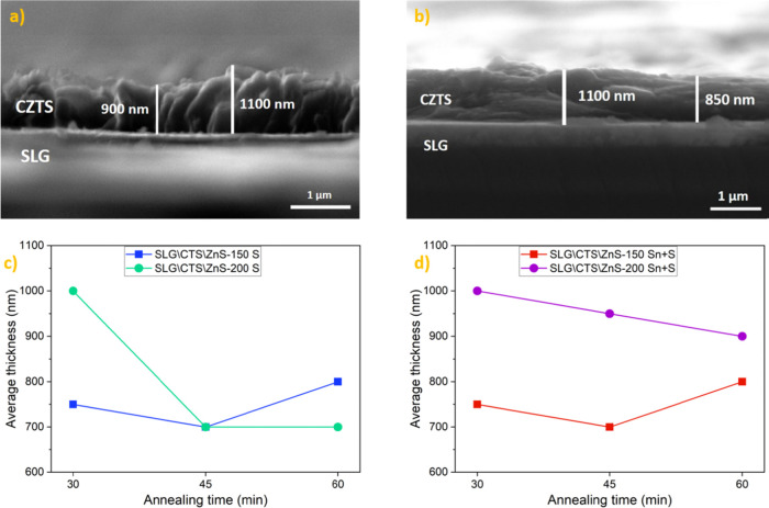
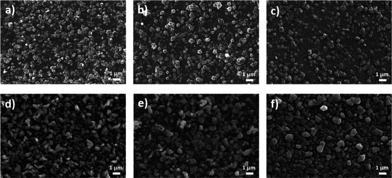
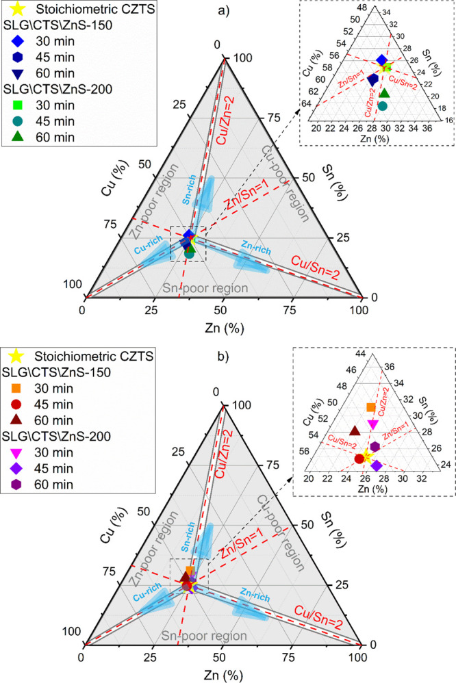
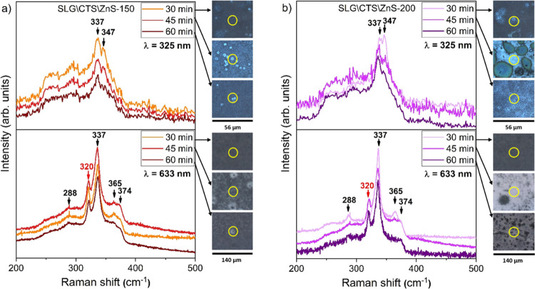
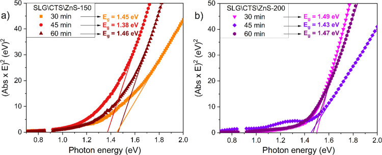
Cu2ZnSnS4 (CZTS) is regarded as one of the emerging materials for next-generation thin film solar cells. However, its synthesis is complex, and obtaining a single-phase CZTS thin film is difficult. This work reports the elaboration of Cu2ZnSnS4 thin films by a sequential magnetron sputtering deposition of Cu2SnS3 (CTS) and ZnS as stacked films. Initially, the CTS films were prepared on a soda lime glass substrate by annealing Cu and SnS2 stacked layers. Second, ZnS was deposited by magnetron sputtering on the CTS films. The CTS\ZnS stacks were then annealed in Sn + S or S atmospheres. The tetragonal CZTS structure was obtained and confirmed by grazing incidence X-ray diffraction and Raman spectroscopy. The morphological and compositional characteristics, measured by scanning electron microscopy and energy-dispersive spectroscopy, revealed large grains and dense surfaces with the elemental composition close to the intended stoichiometry. Additional X-ray photoemission spectroscopy measurements were performed to determine the surface chemistry and particularities of the obtained films. The optical properties, determined using conventional spectroscopy, showed optimal absorber layer band gap values ranging between 1.38 and 1.50 eV. The electrical measurements showed that all the films are p-type with high carrier concentrations in the range of 1015 to 1020 cm-3. This new synthesis route for CZTS opens the way to obtain high-quality films by an industry-compatible method.


Conflict of interest statement

The authors declare no competing financial interest.

Figures

Figure 1
Figure 1
SEM cross-sectional image of (a) SLG\CTS\ZnS-200 sample annealed in S for 30 min and (b) SLG\CTS\ZnS-200 sample annealed in Sn + S for 30 min. The average thickness of the films annealed for 30, 45, and 60 min under (c) S atmosphere and (d) under Sn + S atmosphere.
Figure 2
Figure 2
SEM images of the CZTS films with the SLG\CTS\ZnS-150 stack sulfurized for (a) 30, (b) 45, and (c) 60 min, respectively, and the SLG\CTS\ZnS-200 stack sulfurized for (d) 30, (e) 45, and (f) 60 min, respectively.
Figure 3
Figure 3
SEM images of the CZTS films with the SLG\CTS\ZnS-150 stack annealed in Sn + S atmosphere for (a) 30, (b) 45, and (c) 60 min, respectively; and the SLG\CTS\ZnS-200 stack sulfurized for (d) 30, (e) 45, and (f) 60 min, respectively. The red circles represent grains of the SnS2 secondary phase; the inset in a shows the SnS2 grains observed by EDS mapping.
Figure 4
Figure 4
Ternary phase diagram showing the metallic elemental composition of the CZTS films annealed under (a) S and (b) Sn + S, atmospheres, for different durations, using two ZnS layer thicknesses.
Figure 5
Figure 5
High-resolution spectra for (a) Cu 2p, (b) Zn 2p3/2, (c) Sn 3d5/2, and (d) S 2p for the samples SLG\CTS\ZnS-200 sulfurized for 30 min represented with a blue marker, and for the sample SLG\CTS\ZnS-200 annealed in the Sn + S atmosphere for 60 min represented with a green marker. The black lines are the fit lines while the colored lines represent each individual component.
Figure 6
Figure 6
GIXRD results. (a) ICDD PDF 04-015-0223 of the tetragonal Cu2ZnSnS4 phase. The X-ray diffraction (XRD) patterns of the CZTS films, synthesized using a layer of ZnS, with a thickness of 150 and 200 nm, on top of a CTS layer, annealed for 30, 45, and 60 min in (b) sulfur and (c) tin + sulfur atmospheres. The 101 peak (I = 100) of the ZnS phase (hexagonal, P63mc (186), ICDD PDF 04-012-8144) is indicated with “*,” the 103 peak (I = 100) of the CuS phase (hexagonal, P63/mmc (194), ICDD PDF 04-008-8460) is indicated with “#,” and the 110 peak (I = 100) of the SnS2 phase (hexagonal, P63mc (186), ICDD PDF 00-021-1231) is indicated with “@.”
Figure 7
Figure 7
Unit cell parameters (a and c/2) of the tetragonal CZTS phases in the SLG\CTS\ZnS-150 and SLG\CTS\ZnS-200 samples annealed in (a) S and (b) Sn + S atmospheres for 30, 45, and 60 min. The variation of the unit cell parameters (c) a and (d) c/2, with the mean disorder per Wyckoff position (the sum of the ratio of all defects in the unit cell, divided by 8) obtained from accurate structural data found in the scientific literature (Table 5).
Figure 8
Figure 8
Raman spectra of CZTS films prepared with (a) 150 nm and (b) 200 nm of the ZnS top layer and annealed in the S atmosphere for 30, 45, and 60 min using two different excitation wavelengths (325 and 633 nm). On the right side are shown the relative optical images with the measured spot for each sample.
Figure 9
Figure 9
Raman spectra of CZTS films prepared with (a) 150 nm and (b) 200 nm of the ZnS top layer and annealed in the Sn + S atmosphere for 30, 45, and 60 min using two different excitation wavelengths (325 and 633 nm). On the right side are shown the relative optical images with the measured spot for each sample.
Figure 10
Figure 10
Tauc plots of the CZTS films annealed under the S atmosphere for 30, 45, and 60 min with (a) samples prepared using a 150 nm ZnS top layer and (b) samples prepared using a 200 nm ZnS top layer.
Figure 11
Figure 11
Tauc plots of the CZTS films annealed under the Sn + S atmosphere for 30, 45, and 60 min with (a) samples prepared using a 150 nm ZnS top layer and (b) samples prepared using a 200 nm ZnS top layer.

References

    1. Wang Z.; Demopoulos G. P. Nanoscale Photo-Absorbing Kesterite Grown on Anatase Mesoscopic Films by Sequential Binary Chalcogenide Solution Deposition-Exchange, Annealing, and Etching. Cryst. Growth Des. 2016, 16, 3618–3630. 10.1021/acs.cgd.6b00033. - DOI
    1. Yu K.; Carter E. A. A Strategy to Stabilize Kesterite CZTS for High-Performance Solar Cells. Chem. Mater. 2015, 27, 2920–2927. 10.1021/acs.chemmater.5b00172. - DOI
    1. Azmi S.; Moujib A.; Layachi O. A.; Matei E.; Galca A. C.; Zaki M. Y.; Secu M.; Rusu M. I.; Grigorescu C. E. A.; Khoumri E. M. Towards Phase Pure Kesterite Cu2ZnSnS4 Absorber Layers Growth via Single Step Free Sulfurization Electrodeposition under a Fix Applied Potential on Mo Substrate. J. Alloys Compd. 2020, 842, 15582110.1016/j.jallcom.2020.155821. - DOI
    1. El Khouja O.; Galca A. C.; Zaki M. Y.; Talbi A.; Ahmoum H.; Nouneh K.; Ebn Touhami M.; Taibi M.; Matei E.; Enculescu M.; Pintilie L. Secondary Phases and Their Influence on Optical and Electrical Properties of Electrodeposited Cu2FeSnS4 Films. Appl. Phys. A: Mater. Sci. Process. 2021, 127, 887.10.1007/s00339-021-05038-y. - DOI
    1. Chesman A. S. R.; van Embden J.; Duffy N. W.; Webster N. A. S.; Jasieniak J. J. In Situ Formation of Reactive Sulfide Precursors in the One-Pot, Multigram Synthesis of Cu2ZnSnS4 Nanocrystals. Cryst. Growth Des. 2013, 13, 1712–1720. 10.1021/cg4000268. - DOI