. 2022 Jul 18;13(1):4149.
doi: 10.1038/s41467-022-31886-0.

Low-defect-density WS2 by hydroxide vapor phase deposition

Affiliations

Low-defect-density WS2 by hydroxide vapor phase deposition

Yi Wan et al. Nat Commun. .

Abstract

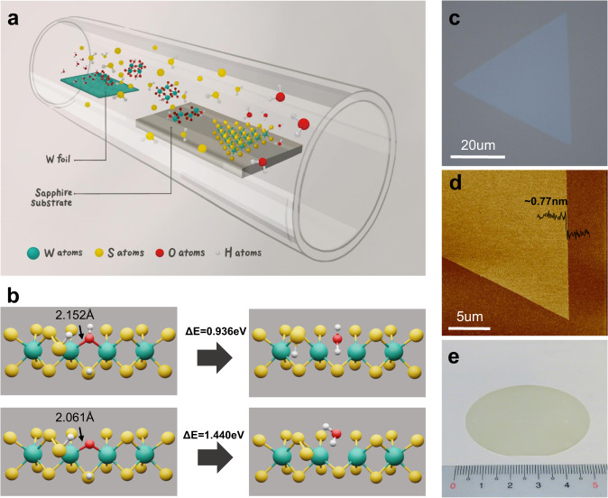
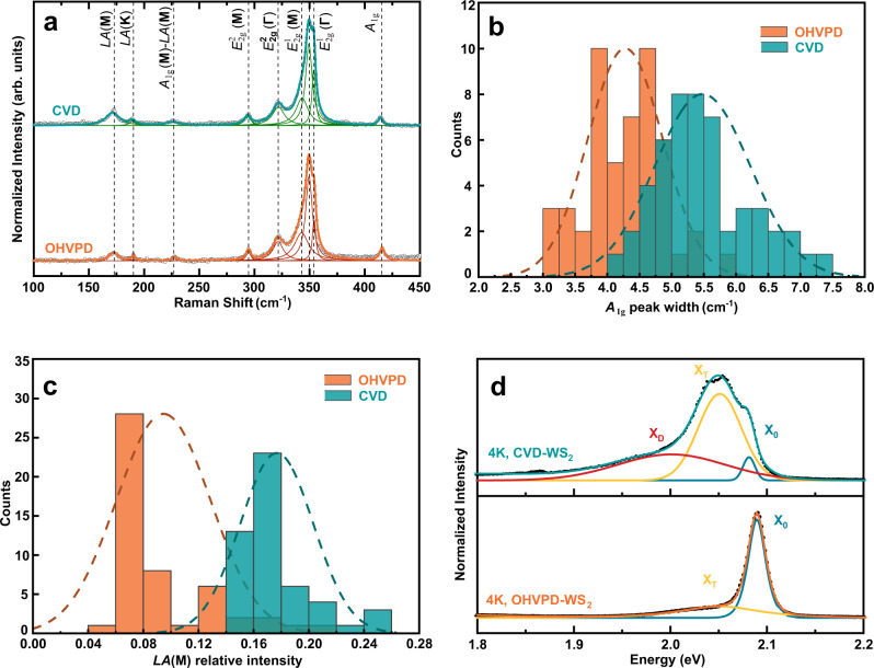
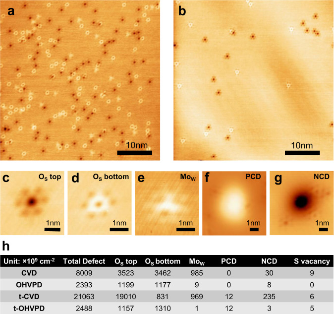
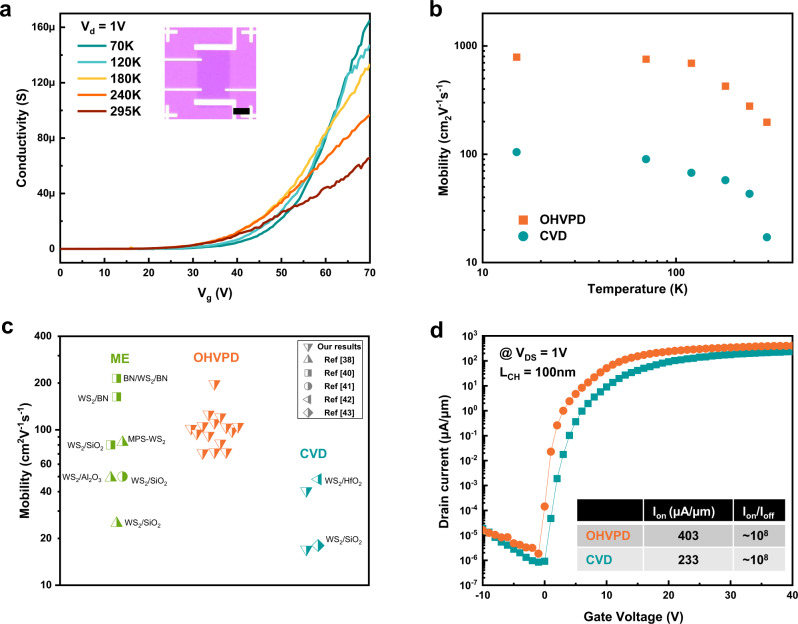
Two-dimensional (2D) semiconducting monolayers such as transition metal dichalcogenides (TMDs) are promising channel materials to extend Moore's Law in advanced electronics. Synthetic TMD layers from chemical vapor deposition (CVD) are scalable for fabrication but notorious for their high defect densities. Therefore, innovative endeavors on growth reaction to enhance their quality are urgently needed. Here, we report that the hydroxide W species, an extremely pure vapor phase metal precursor form, is very efficient for sulfurization, leading to about one order of magnitude lower defect density compared to those from conventional CVD methods. The field-effect transistor (FET) devices based on the proposed growth reach a peak electron mobility ~200 cm2/Vs (~800 cm2/Vs) at room temperature (15 K), comparable to those from exfoliated flakes. The FET device with a channel length of 100 nm displays a high on-state current of ~400 µA/µm, encouraging the industrialization of 2D materials.


Conflict of interest statement

The authors declare no competing interests.

Figures

Fig. 1
Fig. 1. Hydroxide Vapor Phase Deposition.
a Schematic of hydroxide vapor phase deposition (OHVPD) growth of WS2 monolayers. b Nudged elastic band (NEB) simulation of kinetic energy barriers (ΔE) for bonded OH and O dissociating from the edge of WS2. c, d Optical Image c and AFM image d of the OHVPD-WS2 monolayer. e Photo of a 2-inch OHVPD-WS2 monolayer film grown on a sapphire substrate.
Fig. 2
Fig. 2. Optical characterizations of OHVPD- and CVD-WS2 monolayers.
a Typical Raman spectra showing the characteristic modes of OHVPD- and CVD-WS2 monolayers excited by 532 nm wavelengths. The hollow circles and coloured lines are the experimental and Lorentzian fit curves respectively. b, c Statistic distribution of out-of-plane mode A1g Raman peak width and normalized intensity of longitudinal acoustic at M point in the Brillouin zone LA(M) Raman peak for OHVPD- and CVD-WS2 monolayers. The dashed lines represent the normal distribution curves. d Low-temperature PL spectra of OHVPD- and CVD- WS2 monolayers at 4 K. The solid lines and dashed ones are the experimental and fitted peaks respectively. The fitted peaks can be assigned to neutral exciton (X0), trion (XT), and defect-bound exciton (XD).
Fig. 3
Fig. 3. Defect analysis by scanning tunneling microscopy (STM).
a, b STM images of a CVD-WS2 (Bias Voltage (V) = 1.35 V, Current (I) = 40 pA) and b OHVPD-WS2 monolayer (V = 1.15 V, I = 30 pA). cf STM images (V = 1.1 V, I = 30 pA) of the commonly observed point defects in CVD- and OHVPD-WS2: oxygen substituting sulfur (Os) in the c top and d bottom sulfur plane; e Mo substitutional tungsten (MoW); f Positively charged defect (PCD) and g Negatively charged defect (NCD). h, Histograms table of observed point defect density in different OHVPD- and CVD- WS2.
Fig. 4
Fig. 4. Electrical performance of OHVPD-WS2 monolayers.
a Four-probe conductivity as a function of Vg for OHVPD-WS2 monolayer device on the 300 nm SiOx substrate at different temperatures. Insect shows the device structure. (Scale bar: 5 μm) b Field-effect mobility as a function of temperature for OHVPD- and CVD-WS2 monolayers. c Comparison of mobility distribution for our OHVPD-WS2 results (orange), mechanical exfoliation WS2 monolayers (ME, green), and conventional CVD-WS2 (cyan) from literatures. d FET transfer curve of an OHVPD-WS2 monolayer for the short channel device (LCH = 100 nm).

References

    1. Li M-Y, Su S-K, Wong H-SP, Li L-J. How 2D semiconductors could extend Moore’s law. Nature. 2019;567:169–170. doi: 10.1038/d41586-019-00793-8. - DOI - PubMed
    1. Ferain I, Colinge CA, Colinge J-P. Multigate transistors as the future of classical metal–oxide–semiconductor field-effect transistors. Nature. 2011;479:310–316. doi: 10.1038/nature10676. - DOI - PubMed
    1. Chhowalla M, Jena D, Zhang H. Two-dimensional semiconductors for transistors. Nat. Rev. Mater. 2016;1:16052. doi: 10.1038/natrevmats.2016.52. - DOI
    1. Hong J, et al. Exploring atomic defects in molybdenum disulphide monolayers. Nat. Commun. 2015;6:6293. doi: 10.1038/ncomms7293. - DOI - PMC - PubMed
    1. Chu Z, et al. Unveiling defect-mediated carrier dynamics in monolayer semiconductors by spatiotemporal microwave imaging. Proc. Natl Acad. Sci. USA. 2020;117:13908. doi: 10.1073/pnas.2004106117. - DOI - PMC - PubMed