. 2022 Sep;9(27):e2201489.
doi: 10.1002/advs.202201489. Epub 2022 Jul 19.

3D Generation of Multipurpose Atomic Force Microscopy Tips

Affiliations

3D Generation of Multipurpose Atomic Force Microscopy Tips

Ayoub Glia et al. Adv Sci (Weinh). 2022 Sep.

Abstract

In this work, 3D polymeric atomic force microscopy (AFM) tips, referred to as 3DTIPs, are manufactured with great flexibility in design and function using two-photon polymerization. With the technology holding a great potential in developing next-generation AFM tips, 3DTIPs prove effective in obtaining high-resolution and high-speed AFM images in air and liquid environments, using common AFM modes. In particular, it is shown that the 3DTIPs provide high-resolution imaging due to their extremely low Hamaker constant, high speed scanning rates due to their low quality factor, and high durability due to their soft nature and minimal isotropic tip wear; the three important features for advancing AFM studies. It is also shown that refining the tip end of the 3DTIPs by focused ion beam etching and by carbon nanotube inclusion substantially extends their functionality in high-resolution AFM imaging, reaching angstrom scales. Altogether, the multifunctional capabilities of 3DTIPs can bring next-generation AFM tips to routine and advanced AFM applications, and expand the fields of high speed AFM imaging and biological force measurements.

Keywords: 3D printing; carbon nanotubes; focused ion beam; high-resolution imaging; high-speed imaging; polymeric atomic force microscopy tips.


Conflict of interest statement

The authors declare no conflict of interest.

Figures

Figure 1
Figure 1
3D generation of multipurpose AFM tips (3DTIPs). a) CAD design of a 3DTIP showing the mounting base and the array of cantilever‐mounted tips with different geometries. b) Left panel: Schematic showing 2PP working principle for single‐step microfabrication of the 3DTIPs via polymer‐additive manufacturing process. Middle panel, left to right: SEM images reveal that with 2PP, generation of multipurpose 3DTIPs (bead, conical, and HAR) is possible. Scale bars: 25 µm. Right panel: AFM height sensor image, obtained by scanning, in contact mode in air, PS spheres with a conical 3DTIP, reveals high resolution imaging capability. c) Left panel: Schematic showing FIB working principle for etching the tip end of the 3DTIPs. Middle panel: SEM images showing a 3DTIP with enhanced aspect ratio and reduced tip radius. Scale bars: 2 µm and 100 nm (left to right). Right panel: AFM height sensor image, obtained by dynamic scanning plasmid DNA with FIB‐etched 3DTIPs in liquid, reveals enhancement in resolving fine 3D nanostructures. d) Left panel: Schematic showing the steps involved in incorporating the tip end of a 3DTIP with randomly oriented CNTs. Middle panel: SEM images showing the far‐reaching CNTs at the tip end of the CNT‐integrated 3DTIPs. Scale bars: 4 µm and 200 nm (left to right). Right panel: AFM height sensor image, obtained by scanning, in dynamic mode in liquid, pyrolytic graphite with CNT‐integrated 3DTIP in air, reveals the true atomic resolution of its highly ordered structures.
Figure 2
Figure 2
Parametric benchmarking of the 3DTIPs against silicon cantilevers. a) Simulation results for a range of silicon cantilever thicknesses (denoted as t) reveal their first and second oscillation modes. b) In comparison, the simulation results for the 3DTIPs with identical cantilever thicknesses reveal wider range of frequency domain. c) Power spectral density (PSD) shows several oscillation modes for the 3DTIPs, which could be suitable for various AFM measurements. d) For varying cantilever thicknesses, the spring constants of the 3DTIPs are an order of magnitude lower compared to silicon tips, suggesting their use for sensitive force measurements. e) A typical first oscillation mode of a standard silicon tip (t = 0.5 µm) in air. Solid blue line: Lorentzian fit to data. f) The PSD shows the first and second oscillation modes of the 3DTIPs in air with t = 10 µm and t = 2 µm cantilever thicknesses, respectively. g) With the 3DTIPs, obtaining multiple higher oscillation modes in air that span wide tuning range (up to 2 MHz) is possible. h) The PSD shows the first oscillation modes of the 3DTIP with t = 10 µm cantilever thickness in air and liquid. Solid blue line: Lorentzian fit to data.
Figure 3
Figure 3
Imaging quality and tip wear of silicon tips and 3DTIPs in air, as well as 3DTIP durability test in liquid. Top left panels: SEM images of a) standard (pyramidal) silicon tip and b) conical 3DTIP used in characterizing PS spheres (scale bars: 25 µm). Top middle and right panels: AFM height sensor images of 200 nm PS spheres obtained at different scales in air using contact mode. Bottom left panels: Bottom and side views of reconstructed (by deconvolution) tip shapes. Bottom middle and right panels: Full width at half maximum (FWHM) of vertical profiles as a function of size of PS spheres. Box plots represent mean ± SD (n = 28). *: Significantly different at p < 0.05 using two‐sided student's t‐test. c) Left to right: AFM height sensor images of PS spheres with sizes d = 200, 100, 80, 50, and 30 nm obtained with the 3DTIP in air using contact mode. Here, the change in scales of the images is to reveal the deterioration of the resolution with reduced bead sizes. **: The image acquisition was performed in dynamic mode at 86.6 Hz scan rate (1 frame s–1) with 96 × 96 pixel size and 263 × 263 nm2 scanning area. The measured sizes of PS spheres also showed good linear correlation (r 2 > 99) with their manufacturer sizes. Error bars represent mean ± SD (n = 5). d,e) Comparison of AFM height sensor images obtained after first scan and after 12 h continuous scanning of 100 nm PS spheres in air using contact mode revealed that the 3DTIPs are more resistant to tip wear than the silicon tips, also verified by the side views of their reconstructed tip shape images. Notably, compared to the shape of the silicon tip, the shape of the 3DTIP shows excellent tip wear resistance following the imaging. f) AFM amplitude (top) and phase (bottom) images of 200 nm PS spheres obtained with the 3DTIP in liquid using dynamic mode (scan rate = 48.8 Hz) revealed that the 3DTIPs are durable in liquid for prolonged scanning durations.
Figure 4
Figure 4
Imaging of plasmid DNA in liquid with HAR silicon tip and HAR 3DTIP using PeakForce and dynamic mode. SEM images of a) the HAR silicon tip (scale bar: 2 µm) and b) the HAR 3DTIP (scale bar: 10 µm) used in imaging plasmid DNA. The zoomed image in (b) shows the tip shape and size of the 3DTIP (scale bar: 100 nm). c,d) AFM height sensor (top two and bottom left), and bottom right c) adhesion and d) deformation images of plasmid DNA obtained with HAR silicon tip (c) and HAR 3DTIP (d) in liquid using PeakForce mode (scan rate = 24.4 Hz). The height images revealed ≈30 nm apparent thickness of the plasmid DNA. e) AFM phase (top two) and amplitude (bottom two) images of plasmid DNA obtained with HAR 3DTIP in liquid using dynamic mode (scan rate = 24.4 Hz). In phase images, a clear distinction between the DNA and mica is also observed.
Figure 5
Figure 5
High speed imaging performance of conical HAR 3DTIPs (r = 30 nm) in liquid using dynamic mode. a) AFM height sensor images of 50 nm PS spheres obtained by scanning over 263 × 263 nm2 area at 0.2, 1.1, 2.3, and 22 s per frame scan rates, which corresponded to 67.6, 12.3, 5.9, and 0.6 µm s–1 scan speeds, respectively. No visible difference in the shape of PS spheres was observed between the first and 500th scan at 67.6 µm s–1 scan speed. Whereas increasing the scan speed from 0.6 to 12.3 µm s–1 resulted in slight decrease in the quality of images at each pixel. b) AFM height sensor image of 80 nm PS spheres obtained by scanning over 263 × 263 nm2 area at 1 s per frame scan rate, which corresponded to 25.2 µm s–1 scan speed. c) AFM phase images of 30 nm PS spheres obtained by scanning over 500 × 500 nm2 at 0.6, 1.3, and 2.6 s per frame scan rates, which corresponded to 54.6, 25.2, and 12.6 µm s–1 scan speeds, respectively. d) AFM phase (top) and height sensor (middle and bottom) images of 30 nm PS spheres obtained by scanning over 500 × 500 nm2 area at 2.6, 5, and 13 s per frame scan rates, which corresponded to 49.1, 25.6, and 9.8 µm s–1 scan speeds, respectively. e) AFM height sensor images of 30 nm (top) and 50 nm (middle) PS spheres obtained by scanning over 500 × 500 nm2 area at 10.5 and 21 s per frame scan rates, which corresponded to 23.7 and 11.9 µm s–1 scan speeds, respectively. f) AFM height sensor image of 50 nm PS spheres obtained by scanning over 500 × 500 nm2 area at 42 s per frame scan rate, which corresponded to 12.2 µm s–1 scan speed.
Figure 6
Figure 6
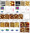
High resolution imaging performance of FIB‐etched and CNT‐integrated 3DTIPs. a,b) SEM images of the FIB‐etched and CNT‐integrated 3DTIPs used in the experiments. Scale bars: (a) 2 µm and 100 nm and (b) 4 µm and 200 nm (left to right). c) AFM phase (top two), adhesion (middle left and bottom), and height sensor (middle right) images obtained at different scales and scan rates with FIB‐etched 3DTIP in liquid using dynamic (top two) and PeakForce (middle two and bottom) modes. The supercoiled DNA (top right) and its plasmid rings (middle right) are revealed, with apparent thickness of ≈4.5 nm. The 3D representation of the plasmid in the adhesion image is also shown in bottom. d) AFM phase images obtained at different scales and scan rates with the CNT‐integrated 3DTIP in liquid using dynamic mode. e) AFM peak force error (top two), height sensor (bottom left), and adhesion (bottom right) images obtained at different scales with CNT‐integrated 3DTIP using PeakForce mode. When compared to performance of FIB‐etched 3DTIP in height sensor image in (c), the apparent plasmid DNA thickness of ≈6.2 nm is revealed in height sensor image in (e). f) The true atomic resolution (with atomic distance of ≈0.3 nm) is achieved on HOPG with CNT‐integrated 3DTIPs in liquid using dynamic mode (scan rate = 24.4 Hz). The hexagonal structure (white circles) and point defects (i.e., voids, the dashed red circle) are resolved. The schematics (bottom) show the highly ordered structure of HOPG. The drawing is not to scale.
Figure 7
Figure 7
Multipurpose 3DTIPs with great flexibility in design and function. Left panel: a–h) SEM and i–m) optical images showing the variety of tip and cantilever shapes in the 3DTIPs that can be generated using 2PP. Depending on the design, the printing time of the 3DTIPs comprising mounting base and five cantilever‐mounted tips can be as low as 35 min to as high as 1.5 h. Clearly, with the proper tip and cantilever design, the AFM applications of 3DTIPs could range from probing forces to high‐resolution, high speed imaging. Scale bars: (a–e) 10 µm, (f–h) 40 µm, (i–k) 120 µm, (l) 30 µm, and (m) 120 µm. Right panel: Magnified SEM images showing the tip end of different HAR 3DTIPs. Scale bars: 100 nm.

Similar articles

Cited by

References

    1. Mou J. X., Sheng S. T., Ho R. Y., Shao Z. F., Biophys. J. 1996, 71, 2213. - PMC - PubMed
    1. Guthold M., Zhu X. S., Rivetti C., Yang G. L., Thomson N. H., Kasas S., Hansma H. G., Smith B., Hansma P. K., Bustamante C., Biophys. J. 1999, 77, 2284. - PMC - PubMed
    1. Butt H. J., Downing K. H., Hansma P. K., Biophys. J. 1990, 58, 1473. - PMC - PubMed
    1. Schabert F. A., Henn C., Engel A., Science 1995, 268, 92. - PubMed
    1. Kasas S., Thomson N. H., Smith B. L., Hansma H. G., Zhu X. S., Guthold M., Bustamante C., Kool E. T., Kashlev M., Hansma P. K., Biochemistry 1997, 36, 461. - PubMed

MeSH terms

Substances

LinkOut - more resources