. 2022 Jul 23;13(1):4266.
doi: 10.1038/s41467-022-31954-5.

Supercurrent diode effect and magnetochiral anisotropy in few-layer NbSe2

Affiliations

Supercurrent diode effect and magnetochiral anisotropy in few-layer NbSe2

Lorenz Bauriedl et al. Nat Commun. .

Abstract

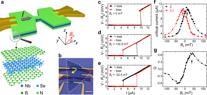
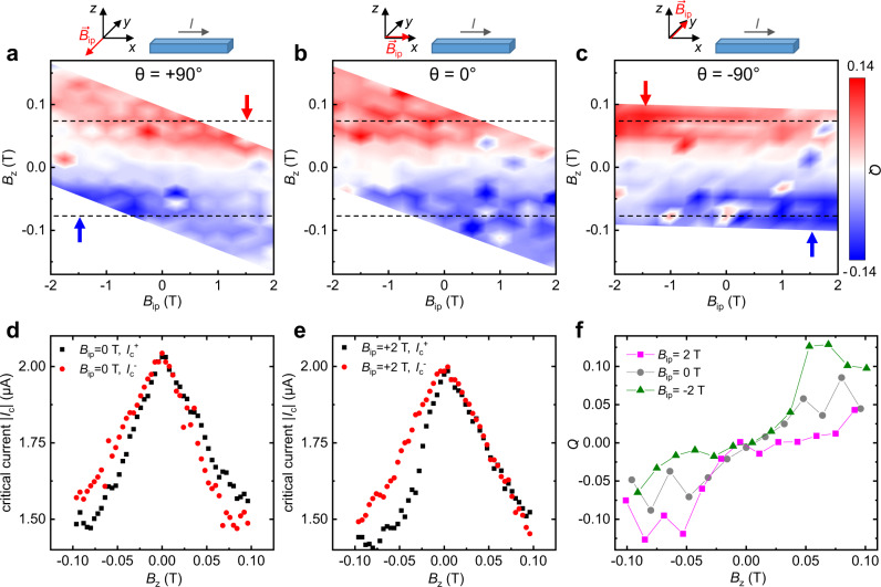
Nonreciprocal transport refers to charge transfer processes that are sensitive to the bias polarity. Until recently, nonreciprocal transport was studied only in dissipative systems, where the nonreciprocal quantity is the resistance. Recent experiments have, however, demonstrated nonreciprocal supercurrent leading to the observation of a supercurrent diode effect in Rashba superconductors. Here we report on a supercurrent diode effect in NbSe2 constrictions obtained by patterning NbSe2 flakes with both even and odd layer number. The observed rectification is a consequence of the valley-Zeeman spin-orbit interaction. We demonstrate a rectification efficiency as large as 60%, considerably larger than the efficiency of devices based on Rashba superconductors. In agreement with recent theory for superconducting transition metal dichalcogenides, we show that the effect is driven by the out-of-plane component of the magnetic field. Remarkably, we find that the effect becomes field-asymmetric in the presence of an additional in-plane field component transverse to the current direction. Supercurrent diodes offer a further degree of freedom in designing superconducting quantum electronics with the high degree of integrability offered by van der Waals materials.


Conflict of interest statement

The authors declare no competing interests.

Figures

Fig. 1
Fig. 1. Supercurrent diode effect in a van der Waals superconductor.
a Scheme of the typical device. The central constriction is 250 nm wide and 250 nm long. The x-direction is chosen to be that of the supercurrent, i.e., the constriction axis. The z-direction is perpendicular to the crystal plane. The device is fabricated starting from a stack of hBN (≈10 nm, tens of layers), NbSe2 (2, 3 or 5 layers) and again hBN (tens of layers). b Optical micrograph of sample B. The dashed white contour highlights the NbSe2 crystal. Electrodes are fabricated by edge contact techniques,,, while the constrictions are made by reactive ion etching. The yellow arrow indicates the supercurrent pathway. The scale bar corresponds to 5 μm. c Current–voltage characteristics (IVs) for opposite bias polarities (i.e., opposite current directions) measured on sample G in a 3-terminal configuration for zero out-of-plane field Bz. The sweep direction is always from zero to finite bias. A contact resistance Rc = 1 kΩ has been subtracted. d Similar measurements, but for Bz = 32.5 mT. Notice the difference between the two critical currents. e Same as in panel (d), but with opposite field orientation. Notice that the role of the two bias polarities now is swapped. f Absolute critical current for positive (black) and negative (red) bias as a function of Bz. Each value is the average of 10 consecutive measurements. The critical current is maximal for a nonzero Bz, namely for Bz=Bmax,Ic10 mT (black and red arrow). The red and black solid line are guides to the eye, mutually symmetric upon reflection around Bz = 0. g Supercurrent rectification efficiency Q2(Ic+Ic)/(Ic++Ic), plotted versus Bz. Q is maximal for Bz=Bmax,Q35 mT (arrow). Measurements in (cg) were performed at 1.3 K. As discussed in the Supplementary Information, an offset of −2.5 mT and 0.17 μA has been removed from Bz and Ic, respectively.
Fig. 2
Fig. 2. Supercurrent diode effect versus in- and out-of-plane field.
a The color plot shows Q2(Ic+Ic)/(Ic++Ic) as a function of out-of-plane (Bz) and in-plane (Bip) field, measured in sample F for θ = 90 (i.e., for BipI). Bz here includes both the field produced by the orthogonal coils and the finite z-component of Bip arising due to misalignment. Red and blue arrows indicate the areas where the diode effect is enhanced. b Similar measurements, but for θ = 0. c As in (b), but for θ = −90. Notice that this graph can be mapped onto that in (a), provided that Bip → −Bip. The color contrast is the same in (a), (b) and (c). d Absolute value of Ic+ (black) and Ic (red) plotted versus Bz, for Bip = 0 and for the sample orientation θ = −90. e As in (d), but for Bip = 2 T. Note that data in (d, e) were measured in a different session (with higher resolution in Bz) compared to data in c. f Supercurrent rectification efficiency Q as a function of Bz at θ = −90 for Bip = −2 T (green), 0 T (gray), and 2 T (magenta). Here, we used the same data as in panel c, for Bip values indicated in the legend. For Bip = 0 we have substituted three outliers (for Bz = −48, −64 and −80 mT) with the corresponding values for the adjacent in-plane field Bip = −0.25 T. For Bip = −2 T we have substituted one outlier (for Bz = −43 mT) with the corresponding value for the adjacent in-plane field Bip = −1.75 T, see Supplementary Information. Outliers are also visible in panels (ac). All measurements reported in this figure were performed at 500 mK.
Fig. 3
Fig. 3. Temperature dependence of the supercurrent diode effect.
The graph shows the temperature dependence of S ≡ Q/Bz for sample D, F, and G. S is evaluated from linear fits of Q(Bz) near Bz = 0, i.e. in the linear regime of the supercurrent rectification efficiency, where Q ∝ Bz. The error bars correspond to the standard error of the fits. The S values are normalized to the lowest temperature value SLT (e.g. 17.2 T−1 for sample G), while the temperatures are normalized to the critical temperature Tc of the corresponding sample. Orange, blue and purple symbols refer to sample D, F and G, where the critical temperature of the constriction region is 4.3 K, 2.25 K and 4.0 K, respectively.

References

    1. Rikken GLJA, Fölling J, Wyder P. Electrical magnetochiral anisotropy. Phys. Rev. Lett. 2001;87:236602. doi: 10.1103/PhysRevLett.87.236602. - DOI - PubMed
    1. Rikken GLJA, Wyder P. Magnetoelectric anisotropy in diffusive transport. Phys. Rev. Lett. 2005;94:016601. doi: 10.1103/PhysRevLett.94.016601. - DOI - PubMed
    1. Ideue T, et al. Bulk rectification effect in a polar semiconductor. Nat. Phys. 2017;13:578. doi: 10.1038/nphys4056. - DOI
    1. Wakatsuki R, et al. Nonreciprocal charge transport in noncentrosymmetric superconductors. Sci. Adv. 2017;3:e1602390. doi: 10.1126/sciadv.1602390. - DOI - PMC - PubMed
    1. Yasuda K, et al. Nonreciprocal charge transport at topological insulator/superconductor interface. Nat. Commun. 2019;10:2734. doi: 10.1038/s41467-019-10658-3. - DOI - PMC - PubMed