Review
. 2022 Jul 13;12(14):2396.
doi: 10.3390/nano12142396.

Review on Perovskite Semiconductor Field-Effect Transistors and Their Applications

Affiliations
Review

Review on Perovskite Semiconductor Field-Effect Transistors and Their Applications

Gnanasampanthan Abiram et al. Nanomaterials (Basel). .

Abstract

Perovskite materials are considered as the most alluring successor to the conventional semiconductor materials to fabricate solar cells, light emitting diodes and electronic displays. However, the use of the perovskite semiconductors as a channel material in field effect transistors (FET) are much lower than expected due to the poor performance of the devices. Despite low attention, the perovskite FETs are used in widespread applications on account of their unique opto-electrical properties. This review focuses on the previous works on perovskite FETs which are summarized into tables based on their structures and electrical properties. Further, this review focuses on the applications of perovskite FETs in photodetectors, phototransistors, light emitting FETs and memory devices. Moreover, this review highlights the challenges faced by the perovskite FETs to meet the current standards along with the future directions of these FETs. Overall, the review summarizes all the available information on existing perovskite FET works and their applications reported so far.

Keywords: field effect transistor; light-emitting FET; mobility; perovskite; photo detector.


Conflict of interest statement

The authors declare no conflict of interest.

Figures

Figure 1
Figure 1
An enormous number of perovskite materials are being used to perform different functions in the thin-film FET literature.
Figure 2
Figure 2
The corner sharing 3D crystal structure of ABX3 perovskite. A⁺ ions embedding the voids of octahedral BX6 by sitting in their cavities.
Figure 3
Figure 3
Classification of the different ionic components formulating the compositions of ABX3 3D perovskites for semiconducting channel materials.
Figure 4
Figure 4
Device structures of perovskite FETs with four different globally recognized configurations (a) bottom gate top contact (BGTC), (b) bottom gate bottom contact (BGBC), (c) top gate bottom contact (TGBC) and (d) top gate top contact (TGTC).
Figure 5
Figure 5
The transfer characteristic curves of the (a) p-channel and (b) n-channel hybrid perovskite-channel-based ambipolar FET. The output characteristics (c) p-channel and (d) n-channel of a triple cation perovskite-channel-based ambipolar FET. Reproduced with the permission from [76]. Copyright 2016 WILEY-VCH Verlag GmbH & Co. KGaA, Weinheim.
Figure 6
Figure 6
Transfer characteristics curve of a perovskite thin film FET with linear and saturated regimes.
Figure 7
Figure 7
Fluorescence microscopy images of (a) MAPbI3, (b) MAPbBr3 and (c) MAPbCl3 single crystals (excited with a pulsed lasers with wavelengths of 450, 473 and 405 nm, respectively) with a scale bar of 100 μm. Inset: optical images of the corresponding single crystals with a scale bar of 200 μm. Schematic of the (d) bottom gate top contact (BGTC) and (e) bottom gate bottom contact (BGBC) device with the tested perovskite single crystal as semiconductor layer and the hole mobility distribution of (20 devices) each halide perovskite under (f) BGTC and (g) BGBC device structure [68], Copyright 2018 Springer Nature.
Figure 8
Figure 8
(a) Transfer characteristics of the typical single VLS−grown CsPbX3 (X = Cl, Br or I) NW FETs using logarithm y-coordinate. Inset shows the SEM image of the as-fabricated NW PD (b) Semilog CsPbBr3 plot of the gate transfer characteristic Ids-Vg measured at Vds = 3.0 V and swipe rate 1.1 V/s. Inset shows the same plot in linear scale. Reproduced with permission from [166]. Copyright 2020, American Chemical Society.
Figure 9
Figure 9
(a) HRTEM image of CsPbBr3 quantum dots (inset: device schematic of the FET) and (b) transfer characteristic curves under different illumination conditions. Reproduced with the permission from (c) [168]. Copyright 2017, Wiley-VCH Verlag GmbH & Co. KGaA, Weinheim. (c) Device schematic of the bilayer FET made-up of CsPbI3 nanorods and C8BTBT, (d) TEM image of CsPbI3 nanorods (e) transfer curves of the FETs under different light intensities [169]. Copyright 2018, Springer Nature. (f) Device schematic along with FET characteristic connections of the CsPbBr3 NCs terminated with short ligands, (g) high- and (h) low-resolution HRTEM image of the CsPbBr3 NCs and transfer characteristic curves of the CsPbBr3 NC FETs under different testing temperatures. Reproduced with permission from, transfer characteristics of undoped CsPbBr3 NCs FETs (i) from 240 to 300 K and (j) 100 to 200 K [83]. Copyright 2020, American Chemical Society.
Figure 10
Figure 10
(a) Device schematic of CH3NH3PbI3 channel-based phototransistor. (b) Transfer characteristics of phototransistor in dark (red and black) and in illumination (blue and magenta) [97]. Copyright 2015, Springer Nature. (c) Device structure with MAPbI3-based photo FET. (d) The hysteresis behaviour and ambipolar transfer characteristics of the photo FET in dark (blue), under 660 nm illumination (orange), under dark again (black). Reproduced with permission from [99]. Copyright 2018, American Chemical Society.
Figure 11
Figure 11
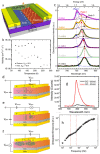
(a) The schematic of the bottom gate bottom contact light emitting FET with CH3NH3PbI3 thin-film channel. (b) Variation in hole and electron mobilities of the same FETs under different operating temperatures and (c) electroluminescence spectra of LEFET under different operating temperatures [20]. Copyright 2015, Springer Nature. The schematics of (d) DC-driven gate and drain fields form a thin recombining region. (e) AC-driven drain field continuously injects the holes and electrons from the drain; (f) both electrons and holes are injected from the source and drain by the applied AC-driven gate voltage used for testing LEFETs. Reproduced with permission from [102]. Copyright 2018 Chemical American Society. (g) The variation in electroluminescence under fixed and pulsed gate bias and integrated emission with the frequency of the voltage pulse applied at gate. (h) Normalized integrated emission of the electroluminescence peaks versus driving voltage frequency. Reproduced with permission from [179]. Copyright 2017 WILEY-VCH Verlag GmbH & Co. KGaA, Weinheim.
Figure 12
Figure 12
(a) Representative output and transfer characteristics of BC/BG transistors (a) without Self Assembled Monolayer (SAM), (b) with NH3I-SAM and (c) TC/TG transistors with NH3I-SAM when measured with forward and reverse scans at a scan rate of 5 Vs−1. Gate currents (Ig), which are correlated with leakage currents occurring through gate dielectrics, are also shown in each Figure. Ig is not so large compared with Id for all of the transistors. Reproduced with permission from [90]. Copyright 2016 WILEY-VCH Verlag GmbH & Co. KGaA, Weinheim. Transfer characteristics of (d) pristine and (e) 2% urea-added (PEA)2SnI4 perovskite-based FETs and (f) their current stability over time. Reproduced with permission from [175]. Copyright 2021 Elsevier Ltd.
Figure 13
Figure 13
(a) Transfer curves of MAPbI3-based FET at various temperatures between 150 K and 250 K [94]. (b) Evolution of ON and OFF currents as a function of time, where the devices were kept in the dark with a relative humidity between 40% and 60% over a period of 2 months in ambient atmosphere. Reproduced with permission from [196]. Copyright 2020, American Chemical Society. (c) Evolution of hole mobilities of the BGTC FET devices based on (PEA)2SnI4 and (4Tm)2SnI4 over a long storage time. Reproduced with the permission from [157]. Copyright 2019, American Chemical Society.
Figure 14
Figure 14
Distribution of hole mobility of various perovskite materials studied using FET structure.

References

    1. Deschler F., Neher D., Schmidt-Mende L. Perovskite semiconductors for next generation optoelectronic applications. APL Mater. 2019;7:7–10. doi: 10.1063/1.5119744. - DOI
    1. Fu Y., Zhu H., Chen J., Hautzinger M.P., Zhu X.Y., Jin S. Metal halide perovskite nanostructures for optoelectronic applications and the study of physical properties. Nat. Rev. Mater. 2019;4:169–188. doi: 10.1038/s41578-019-0080-9. - DOI
    1. Rhee S., An K., Kang K.T. Recent advances and challenges in halide perovskite crystals in optoelectronic devices from solar cells to other applications. Crystals. 2021;11:39. doi: 10.3390/cryst11010039. - DOI
    1. Rezaee E., Kutsarov D., Li B., Bi J., Silva S.R.P. OPEN A route towards the fabrication of large-scale and high-quality perovskite films for optoelectronic devices. Sci. Rep. 2022;12:7411. doi: 10.1038/s41598-022-10790-z. - DOI - PMC - PubMed
    1. Hao J., Xiao X. Recent Development of Optoelectronic Application Based on Metal Halide Perovskite Nanocrystals. Front. Chem. 2022;9:822106. doi: 10.3389/fchem.2021.822106. - DOI - PMC - PubMed

LinkOut - more resources