. 2022 Jul 24;13(8):1169.
doi: 10.3390/mi13081169.

Compensation of the Stress Gradient in Physical Vapor Deposited Al1-xScxN Films for Microelectromechanical Systems with Low Out-of-Plane Bending

Affiliations

Compensation of the Stress Gradient in Physical Vapor Deposited Al1-xScxN Films for Microelectromechanical Systems with Low Out-of-Plane Bending

Rossiny Beaucejour et al. Micromachines (Basel). .

Abstract

Thin film through-thickness stress gradients produce out-of-plane bending in released microelectromechanical systems (MEMS) structures. We study the stress and stress gradient of Al0.68Sc0.32N thin films deposited directly on Si. We show that Al0.68Sc0.32N cantilever structures realized in films with low average film stress have significant out-of-plane bending when the Al1-xScxN material is deposited under constant sputtering conditions. We demonstrate a method where the total process gas flow is varied during the deposition to compensate for the native through-thickness stress gradient in sputtered Al1-xScxN thin films. This method is utilized to reduce the out-of-plane bending of 200 µm long, 500 nm thick Al0.68Sc0.32N MEMS cantilevers from greater than 128 µm to less than 3 µm.

Keywords: MEMS; aluminum scandium nitride; cantilever beams; fabrication; physical vapor deposition; stress; stress gradient.


Conflict of interest statement

The authors declare no conflict of interest.

Figures

Figure 1
Figure 1
Fabrication process for realizing Al1−xScxN cantilevers with (a) p-type (100) Si wafer (b) Al1−xScxN deposition using Evatec CLUSTERLINE® 200 II PVD system (c) PECVD SiN deposition and patterning using CF4 RIE (d) KOH in 45% H2O etch of Al1−xScxN (e) SiN hard mask stripped using CF4 RIE and Al1−xScxN cantilevers released using isotropic XeF2 dry etching.
Figure 2
Figure 2
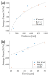
Average stress plots of PVD deposited Al0.68Sc0.32N films with (a) Average stress versus thickness plot at a constant 25 sccm N2 flow and (b) Average stress versus flow for 500 nm Al0.68Sc0.32N with pure N2 flow from 20–30 sccm [3].
Figure 3
Figure 3
Graphics for a 500 nm PVD sputter-deposited Al0.68Sc0.32N film where the N2 process gas flow is held constant through the entire deposition, (a) 45-degree SEM image of center die (C) fabricated from a 100 mm wafer. Each die has 8 released structures which are labeled. Note the high out-of-plane deflection that is clearly visible in the uncompensated structures. (b) Schematic of locations on the 100 mm wafer where a die is pulled 35 mm from the center for imaging and measuring out-of-plane displacements. One die was pull from the north (N), northeast (NE), east (E), southeast (SE), south (S), southwest (SW), west (W), and northwest (NW) locations of the wafer (c) Stack-up of film with constant flow composed of a seed layer, gradient seed layer (Al1→0.68Sc0→0.32N) [3] and Al0.68Sc0.32N layer.
Figure 4
Figure 4
(ai) SEM images of cantilevers formed from 500 nm thick PVD Al0.68Sc0.32N films deposited under a constant N2 flow of 25 sccm. Each die was pulled from the north (N), northeast (NE), east (E), southeast (SE), south (S), southwest (SW), west (W), and northwest (NW) locations of the wafer shown in Figure 3b.
Figure 5
Figure 5
Graphics for multi-layer 500 nm PVD sputter-deposited Al0.68Sc0.32N film where the N2 process gas flow is changed between two layers with 30 sccm utilized on the bottom and 25 sccm on the top layer, (a) 45-degree SEM image of the center die (C) fabricated from a 100 mm wafer. Each die has 8 released structures. (b) Stack-up of 2-layer film composed of a seed and gradient layer (Al1→0.68Sc0→0.32N) [3] to suppress AOGs and two equal thickness layers with different N2 process gas flows designed to compensate for the native through-thickness stress gradient.
Figure 6
Figure 6
Graphics for multi-layer 500 nm PVD sputter-deposited Al0.68Sc0.32N film, (a) 45-degree SEM image of the center die (C) fabricated from a 100 mm wafer. (b) Stack-up with five equal thickness layers with different N2 process gas flows to compensate for the through-thickness stress gradient.
Figure 7
Figure 7
Top view SEM images of cantilevers formed from a 5-layer, 500 nm total thickness, PVD deposited Al0.68Sc0.32N where the process gas flow for each layer is linearly changed from 30 to 20 sccm through the five layers. Each die was pull from the north (N), northeast (NE), east (E), southeast (SE), south (S), southwest (SW), west (W), and northwest (NW) locations of the wafer shown in Figure 3b.
Figure 8
Figure 8
Z deflection for 500 nm PVD sputter-deposited Al0.68Sc0.32N films where the N2 process gas flow was applied at constant flow throughout the deposition (black) and a 2-layer 30/20 sccm N2 flow stack (red).

References

    1. Esteves G., Berg M., Wrasman K.D., Henry M.D., Griffin B.A., Douglas E.A. CMOS compatible metal stacks for suppression of secondary grains in Sc0.125Al0.875N. J. Vac. Sci. Technol. A Vac. Surf. Film. 2019;37:021511. doi: 10.1116/1.5065517. - DOI
    1. Olsson R.H., Tang Z., D’Agati M. Doping of aluminum nitride and the impact on thin film piezoelectric and ferroelectric device performance; Proceedings of the 2020 IEEE Custom Integrated Circuits Conference (CICC); Boston, MA, USA. 22–25 March 2020; New York, NY, USA: IEEE; 2020. pp. 1–6.
    1. Beaucejour R., Roebisch V., Kochhar A., Moe C., Hodge D., Olsson R.H., III Controlling Residual Stress and Suppression of Anomalous Grains in Aluminum Scandium Nitride Films Grown Directly on Silicon. [(accessed on 1 June 2022)];J. Microelectromech. Syst. 2022 :1–8. doi: 10.1109/JMEMS.2022.3167430. Available online: https://ieeexplore.ieee.org/document/9770129. - DOI
    1. Hong Y., Sui L., Zhang M., Shi G. Theoretical analysis and experimental study of the effect of the neutral plane of a composite piezoelectric cantilever. Energy Convers. Manag. 2018;171:1020–1029. doi: 10.1016/j.enconman.2018.06.045. - DOI
    1. Wang Q.M., Yang Z., Li F., Smolinski P. Analysis of thin film piezoelectric microaccelerometer using analytical and finite element modeling. Sens. Actuators Phys. 2004;113:1–11. doi: 10.1016/j.sna.2004.02.041. - DOI

LinkOut - more resources