. 2022 Aug 4;12(1):13449.
doi: 10.1038/s41598-022-17648-4.

An ultra-wideband origami microwave absorber

Affiliations

An ultra-wideband origami microwave absorber

Akash Biswas et al. Sci Rep. .

Abstract

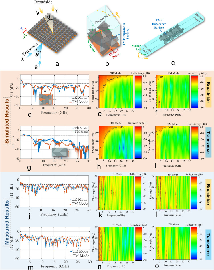
Microwave absorbers have been used to mitigate signal interference, and to shield electromagnetic systems. Two different types of absorbers have been presented: (a) low-cost narrowband absorbers that are simple to manufacture, and (b) expensive wideband microwave absorbers that are based on complex designs. In fact, as designers try to increase the bandwidth of absorbers, they typically increase their complexity with the introduction of several electromagnetic components (e.g., introduction of multi-layer designs, introduction of multiple electromagnetic resonators, etc.,), thereby increasing their fabrication cost. Therefore, it has been a challenge to design wideband absorbers with low cost of fabrication. To address this challenge, we propose a novel design approach that combines origami math with electromagnetics to develop a simple to manufacture ultra-wideband absorber with minimal fabrication and assembly cost. Specifically, we utilize a Tachi-Miura origami pattern in a honeycomb configuration to create the first absorber that can maintain an absorptivity above 90% in a 24.6:1 bandwidth. To explain the ultra-wideband behavior of our absorber, we develop analytical models based on the transmission-reflection theory of electromagnetic waves through a series of inhomogeneous media. The ultra-wideband performance of our absorber is validated and characterized using simulations and measurements.


Conflict of interest statement

The authors declare no competing interests.

Figures

Figure 1
Figure 1
Next-generation communication systems in smart cities.
Figure 2
Figure 2
Schematic diagram of media coated with a resistive layer of Zink impedance. (a) Homogeneous medium with one dielectric layer. (b) Inhomogeneous medium with two dielectric layers and one air layer.
Figure 3
Figure 3
(a) Analytically calculated reflection coefficient for the 1-layer homogeneous and 2-layer inhomogeneous media, (b) dielectric media studied using simulation, and (c) simulated reflection coefficient for the media cases in Fig. 3b.
Figure 4
Figure 4
Effective material homogenization analysis of the dielectric structure of our TMP absorber (no metal and resistive layers are included). (a) Perspective and top views of our TMP absorber, and its equivalent homogenized model for wall thickness t = 4 mm. A step-by step design process for the 3D structure of our TMP absorber is presented in Figs. S4 and S5 of our Supplementary Material in Section 2.2. (b) Volume fill factor, g, response as the wall thickness, t, varies from 0 to 6 mm. (c) Relationship between εt and volume fill factor, g. (d) Evaluated reflection coefficients of TMP absorber following different approaches. (e) Perspective and top views of a honeycomb unit cell. (f) Reflection coefficients of the honeycomb and TMP unit cell.
Figure 5
Figure 5
(a) A 10×10.5 unit cell array of our proposed TMP absorber. Simulation setup of the TMP absorber unit cell for: (b) broadside illumination, and (c) transverse illumination. Simulated reflectivity of TMP absorber for TE and TM modes with respect to the structure shown in the inset for: (d) broadside illumination and an incidence wave angle of θ=0, and (g) transverse illumination and an incidence wave angle of (ϕ=0 and θ=90). Simulated reflectivity of TMP absorber for different angles of incidence for broadside illumination: (e) TE mode, (f) TM mode. Simulated reflectivity of TMP absorber for different angles of incidence for transverse illumination: (h) TE mode, and (i) TM mode. Measured reflectivity of TMP absorber for TE and TM modes for: (j) broadside, and (m) transverse illumination cases. Measured reflectivity of TMP absorber for different angles of incidence for broadside illumination: (k) TE mode, (l) TM mode. Measured reflectivity of TMP absorber for different angles of incidence for transverse illumination: (n) TE mode, and (o) TM mode.
Figure 6
Figure 6
(a) A 2×2 TMP array. Each color shows the outline of a different TMP unit cell. (b) The rectangular area that the 5 TMP array occupies is shown by the blue box. (c) The parameters of a regular hexagonal honeycomb unit cell. a is the side length of the hexagon. All other dimensions are defined in relation to this parameter. (d) The area that the 5 hexagon array occupies is shown by the blue box. The width and height dimensions of the box are shown in terms of the sidelength, a, of the hexagon. (e) The principal directions used for the mechanical analysis of the TMP and Hexagonal Honeycomb. The origin of the TMP is located at the center of the front crease. The origin of the hexagonal honeycomb is located at the center of the hexagonal honeycomb. Subfigures (f)–(h) show the loading conditions on 14 of the TMP and 18 of the hexagonal honeycomb. (f) The loading conditions in the x-direction. The deflection was applied on the orange edge in the positive x-direction. (g) The loading conditions in the y-direction. The deflection was applied on the front face in the positive y-direction. A rigid support was placed on the back face, shown in lighter red. (h) The loading conditions in the z-direction. The deflection was applied on the bottom edge, shown in blue, in the positive z-direction. The green dashed lines show where the frictionless supports were applied to each honeycomb structure. The lighter green area shows a frictionless support on the opposite side to the panel view.
Figure 7
Figure 7
Force-deflection trends for the Tachi–Miura Polyhedron and Hexagonal Honeycombs with Aramid material properties in the x, y, and z directions for the different material thicknesses. (a) The x-direction force-deflection curves. (b) The y-direction force-deflection curves. (c) The z-direction force-deflection curves. (d) A comparison of the 5 mm thick TMP and Hexagonal honeycombs’ force-deflection responses in the x, y, and z-directions. The solid lines represent the TMP force-deflection behavior and the dashed lines represent the Hexagonal honeycomb force-deflection behavior. The ‘×’ shows the initial yield point for the TMP. The ‘’ shows the initial yield point for the hexagonal honeycomb. The hexagon shape shows the location where the average stress is at the yield stress for the TMP honeycomb. The triangle shape (‘’) shows the location where the average stress is at the yield stress for the Hexagonal honeycomb.
Figure 8
Figure 8
Fabrication process of the TMP absorber: (a) cardstock paper is scored using a Silhouette Cameo, (b) scored flat front panel, (c) C-808 conductive carbon ink, (d) spraying ink with airbrush, (e) curing in the oven, (f) folding flat panel, (g) several folded panels joined together, and (h) prototype of TMP absorber inside a box frame. Measurement setup of our proposed absorber: (i) Schematic of setup. (j) Setup used for calibration. (k) Setup for broadside illumination with the TE mode at an incident angle of θ=60. (l) Setup for transverse illumination with the TE mode at an incident angle of θ=0; our absorber is shown in the inset view.

References

    1. Ghosh A, Maeder A, Baker M, Chandramouli D. 5g evolution: A view on 5g cellular technology beyond 3g pp release 15. IEEE Access. 2019;7:127639–127651. doi: 10.1109/ACCESS.2019.2939938. - DOI
    1. Calvanese Strinati E, et al. 6g: The next frontier: From holographic messaging to artificial intelligence using subterahertz and visible light communication. IEEE Veh. Technol. Mag. 2019;14:42–50. doi: 10.1109/MVT.2019.2921162. - DOI
    1. Salisbury, W. W. Absorbent body for electromagnetic waves. US Patent 2599944A (1952).
    1. Sun L, Cheng H, Zhou Y, Wang J. Design of a lightweight magnetic radar absorber embedded with resistive FSS. IEEE Antennas Wirel. Propag. Lett. 2012;11:675–677. doi: 10.1109/LAWP.2012.2203292. - DOI
    1. Costa F, Monorchio A, Manara G. Theory, design and perspectives of electromagnetic wave absorbers. IEEE Electromagn. Compat. Mag. 2016;5:67–74. doi: 10.1109/MEMC.0.7543954. - DOI