. 2022:2022:9870386.
doi: 10.34133/2022/9870386. Epub 2022 Jun 30.

Highly Integrated Multiplexing and Buffering Electronics for Large Aperture Ultrasonic Arrays

Affiliations

Highly Integrated Multiplexing and Buffering Electronics for Large Aperture Ultrasonic Arrays

Robert Wodnicki et al. BME Front. 2022.

Erratum in

Abstract

Large aperture ultrasonic arrays can be implemented by tiling together multiple pretested modules of high-density acoustic arrays with closely integrated multiplexing and buffering electronics to form a larger aperture with high yield. These modular arrays can be used to implement large 1.75D array apertures capable of focusing in elevation for uniform slice thickness along the axial direction which can improve image contrast. An important goal for large array tiling is obtaining high yield and sensitivity while reducing extraneous image artifacts. We have been developing tileable acoustic-electric modules for the implementation of large array apertures utilizing Application Specific Integrated Circuits (ASICs) implemented using 0.35 μ m high voltage (50 V) CMOS. Multiple generations of ASICs have been designed and tested. The ASICs were integrated with high-density transducer arrays for acoustic testing and imaging. The modules were further interfaced to a Verasonics Vantage imaging system and were used to image industry standard ultrasound phantoms. The first-generation modules comprise ASICs with both multiplexing and buffering electronics on-chip and have demonstrated a switching artifact which was visible in the images. A second-generation ASIC design incorporates low switching injection circuits which effectively mitigate the artifacts observed with the first-generation devices. Here, we present the architecture of the two ASIC designs and module types as well imaging results that demonstrate reduction in switching artifacts for the second-generation devices.


Conflict of interest statement

Conflicts of Interest R.W., Q.Z., D.N.S., and K.W.F. have patents and/or patent applications that include aspects of the research presented in this paper. The other authors declare no conflict of interest.

Figures

Figure 1
Figure 1
Illustration of a large aperture ultrasonic array which has benefits for imaging of deep lesions for cancer diagnosis and screening. These include improved contrast due to electronic focus in elevation and improved lateral resolution due to a reduced F#.
Figure 2
Figure 2
Illustration of different multiplexing and buffering architectures and parasitic effects. (a) First-generation ASICs with a single buffer and high voltage select switch (red); each buffer has a high voltage transmit/receive switch (not shown) that effectively makes this path bidirectional, (b) single-unit cell, (c) second-generation ASIC modules with single buffers (and T/R switch, not shown) off-chip at top of each column, (d) effects of parasitics when multiple ASICs with on-chip buffers are ganged together, and (e) multiple ASICs with off-chip buffers.
Figure 3
Figure 3
The first- (a, b) and second- (c, d) generation ASICs incorporating multiple mux switches for interfacing to 2D and 1.75D transducer array elements. (a) First-generation ASIC unit cell, (b) complete first-generation device, (c) complete second-generatation ASIC, (d) second-generation ASIC unit cell CAD layout ((b) adapted from [30], (c-d) adapted from [40]).
Figure 4
Figure 4
Schematic representation of the ASIC unit cells. (a) First-generation with integrated buffer, illustrating the transmit/receive protection high voltage switches (TX, RX1, and RX2) as well as the matrix multiplexing switch (SEL), and digital data storage D flip-flop connected to DIN, (b) small signal circuit model for (a), (c) second-generation ASIC unit cell without buffer and transmit/receiving circuit, (d) small-signal circuit model for (c), operation of the unit cell of (a) when (e) deselected, (f) selected in transmit mode, and (g) selected in receive mode. The red arrows show the transmit signal path, while the green arrows show the receive signal path.
Figure 5
Figure 5
Timing diagram for operation of the unit cell circuitry of Figure 4. The circuit operates in separate TX and RX states, with the TX switch being enabled during the TX state and the two RX switches being enabled during the RX state. This effectively serves to route high voltage signals around the amplifier while also removing the low impedance feedback path of the TX switch during the RX state.
Figure 6
Figure 6
ASIC unit cell layouts: (a) first-generation device and (b) second-generation device.
Figure 7
Figure 7
Switch architecture for the first- and second-generation switches. All switches used in each respective unit cell (e.g., select and transmit/receive) utilize these basic architectures. The second-generation switches have source resistors R1 and R2 which reduce the current in the mirrors and thereby slow down charging of the switch device gate capacitances (M1/M2) to limit charge-injection. (b) adapted from [31].
Figure 8
Figure 8
Simulation results for the unit switch. The switch operates in DYNAMIC and STATIC modes: In the STATIC precharge mode, the gates of M1/M2 are charged to a low voltage to turn them ON. Then, in the DYNAMIC mode, the gates float which allow the switch to conserve power and enables high voltage signals to pass through the devices M1 and M2 without damaging their sensitive low voltage gates.
Figure 9
Figure 9
Receive frequency response of the unit cells, (a) model (Equation (1)) comparison of first-generation response when loaded with ultrasound cable (100 pF case) vs. unloaded (10 pF case) as with a PCB connection, and (b) plots of the models of Equation (1) and Equation (2) as compared to actual measured data with the first- and second-generation ASIC modules utilizing a 16 pF series capacitance and function generator as a source load model of the transducers in receive mode.
Figure 10
Figure 10
Integration of first- and second-generation ASICs with respective acoustic stacks. (a) first-generation module, (b) second-generation module including MAX4805 receive buffers ((a) adapted from [30] (b) from [31]).
Figure 11
Figure 11
Validation of electrical function of the first-generation ASICs. (a) receive test and (b) high voltage switch test.
Figure 12
Figure 12
The parasitic capacitances at the inputs of the first- and second-generation modules were determined using the circuits in (a) for first- and (b) for second-generation devices. The table in (c) shows calculated values for first- and second-generation with increasing N. The final value for Cpn was calculated as the mean of the 4 measured values.
Figure 13
Figure 13
Transmit ON resistance of the individual ASIC module channels was measured as illustrated in (a) for the first-generation architecture and (b) for the second-generation device. The attenuation, α, is visible in (c) where the red trace is the input signal and the purple trace is the attenuated voltage measured across RTest. Calculated RTransmit values for first- and second-generation are tabulated in (d).
Figure 14
Figure 14
The transmit off-isolation was measured by operating the first- and second-generation modules interfaced to the Verasonics system with a single cycle pulse at 38 Vpp and Fc=3.5MHz. (a) shows the result when the switch is ON, and (b) shows the result when the switch is OFF. As can be seen in (b), the transmitted pulse is effectively reduced by 46 dB with the switch turned off, and (c) tabulates these results.
Figure 15
Figure 15
Measurement of Glitch level. (a) Verasonics receive signal with arrow indicating the glitch echo, (d) analogous voltage oscilloscope trace measurement, with arrow indicating observed outgoing glitch waveform (pink trace) in response to digital control signal (green trace) that turns on the switch. Translating control signal (e) moves the glitch response (arrow in (b)). (c) When transmit pulses are turned off, the acoustic response prior to the glitch disappears; however, the glitch itself is unchanged indicating that it is caused by switching transients.
Figure 16
Figure 16
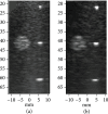
Acoustic imaging tests for the (a) first- and (b) second-generation acoustic/ASIC modules imaging a highly echogenic cyst and a vertical group of wires in a CIRS 054GS ultrasound phantom. Displayed dynamic range for the images was 40 dB.
Figure 17
Figure 17
Glitch reduction in second-generation devices when imaging quartz target, (a) first-generation ASIC module (b) second generation ASIC module, arrows show the location of the image artifact due to glitches (c-d) show plots of the Verasonics RF receive data for (c) the first-generation and (d) the second generation ASIC mdoules, arrows indicate where the glitches are located. (adapted from [31]).

References

    1. Hoskins P. R., Martin K., and Thrush A.. Diagnostic Ultrasound: Physics and Equipment, Cambridge University Press, 2010
    1. Shung K. K.Diagnostic Ultrasound: Imaging and Blood Flow Measurements, CRC Press, Second, 2015
    1. Otto C. M.The practice of clinical echocardiography, Elsevier Health Sciences, 2007
    1. Fernandez A. T., Gammelmark K. L., Dahl J. J., Keen C. G., Gauss R. C., and Trahey G. E., “Synthetic elevation beamforming and image acquisition capabilities using an 8 x 128 1.75D array,” IEEE Transactions on Ultrasonics, Ferroelectrics, and Frequency Control, vol. 50, no. 1, pp. 40–57, 2003 - PubMed
    1. Tamano S., Yamazaki M., Sano S., Hara K., Sakano J., and Miwa Y., “3D ultrasound imaging system using Fresnel ring array,” IEEE symposium on Ultrasonics, vol. 2, pp. 1310–1313, 2003