. 2022 Jun 23:2022:9767651.
doi: 10.34133/2022/9767651. eCollection 2022.

Realization of Oriented and Nanoporous Bismuth Chalcogenide Layers via Topochemical Heteroepitaxy for Flexible Gas Sensors

Affiliations

Realization of Oriented and Nanoporous Bismuth Chalcogenide Layers via Topochemical Heteroepitaxy for Flexible Gas Sensors

Zhiwei Wang et al. Research (Wash D C). .

Abstract

Most van der Waals two-dimensional (2D) materials without surface dangling bonds show limited surface activities except for their edge sites. Ultrathin Bi2Se3, a topological insulator that behaves metal-like under ambient conditions, has been overlooked on its surface activities. Herein, through a topochemical conversion process, ultrathin nanoporous Bi2Se3 layers were epitaxially deposited on BiOCl nanosheets with strong electronic coupling, leading to hybrid electronic states with further bandgap narrowing. Such oriented nanoporous Bi2Se3 layers possessed largely exposed active edge sites, along with improved surface roughness and film forming ability even on inkjet-printed flexible electrodes. Superior room-temperature NO2 sensing performance was achieved compared to other 2D materials under bent conditions. Our work demonstrates that creating nanoscale features in 2D materials through topochemical heteroepitaxy is promising to achieve both favorable electronic properties and surface activity toward practical applications.


Conflict of interest statement

The authors declare no conflicts of interest.

Figures
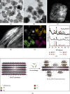
Figure 1
Figure 1
TEM images of (a) BiOCl nanosheets and (b) Bi2Se3/BiOCl heterostructures. (c) STEM image of a Bi2Se3/BiOCl heterostructure, revealing a nanoporous Bi2Se3 layer with a pore size of 1-3 nm. (d) Side-view STEM image of Bi2Se3/BiOCl heterostructures. (e) STEM image and EDX mapping of Bi2Se3/BiOCl heterostructures. (f) XRD patterns of BiOCl nanosheets and Bi2Se3/BiOCl heterostructures. (g) Schematic illustration of the formation process of the Bi2Se3/BiOCl heterostructure.
Figure 2
Figure 2
(a) SAED pattern of a Bi2Se3/BiOCl heterostructure. The pattern for BiOCl with a fourfold symmetry is indicated by a yellow square; two patterns for Bi2Se3 with a sixfold symmetry are indicated by red and green hexagons. (b) HRTEM image of an area with overlapping lattices of BiOCl and Bi2Se3. Inset: the corresponding FFT diffraction pattern. (c) BiOCl [001]-zone and (d) Bi2Se3 [001]-zone lattice patterns generated by performing inverse-FFT of the spots forming the red hexagon and the yellow square in (b), respectively. Insets in (c and d): the selected spots. (e) Schematic top-view and side-view models indicating the BiOCl (001) || Bi2Se3 (001) and BiOCl [100] || Bi2Se3 [110] epitaxial relationship. Side-view HRTEM images of typical Bi2Se3/BiOCl heterostructures with (f) 1 QL and (g) 2 QLs Bi2Se3 grown on a BiOCl nanosheet.
Figure 3
Figure 3
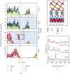
(a) Calculated PLDOS of Bi2Se3 (the top 1st panel) and BiOCl (bottom panel) before and after (the 2nd and 3rd panels) contact. (b) Calculated structure model of the Bi2Se3-BiOCl interface superimposed with the charge density difference (cyan: positive; pink: negative). (c) Raman spectra of BiOCl, Bi2Se3, and Bi2Se3/BiOCl heterostructures.
Figure 4
Figure 4
(a) Dynamic response-recovery curve of the sensor fabricated from Bi2Se3/BiOCl heterostructures in response to NO2 gas with increasing gas concentration at room temperature. (b) Sensing response vs. NO2 concentration for BiOCl-, Bi2Se3-, and Bi2Se3/BiOCl-based sensors. (c) Response of Bi2Se3/BiOCl heterostructures upon exposure to 10 ppm NO2, H2S, C7H8, C2H5OH, NH3, (CH3)2CO, CO2, and HCHO at room temperature. (d) Sensing response vs. NO2 concentration for Bi2Se3/BiOCl-based sensor with and without a 365 nm light irradiation (8.31 μW).
Figure 5
Figure 5
(a) Calculated structural models of NO2 molecules absorbed on the BiOCl (001), Bi2Se3 (001), (100), and (110) surfaces. (b) Calculated adsorption energy (eV) and electron transferred (e) toward NO2 on different sensing surfaces. HRTEM images showing the (c) (110) edge plane and (d) (100) edge plane of Bi2Se3.
Figure 6
Figure 6
(a) Schematic diagram of the Bi2Se3/BiOCl heterostructures on flat and bent substrates. (b) Responses of Bi2Se3/BiOCl-based sensors under flat and bent states at various NO2 concentrations. Inset: a photograph of the printed electrode array. (c) Comparison of the sensing performance between our flexible gas sensor and other 2D material-based flexible sensors under bending conditions.

Similar articles

Cited by

References

    1. Jin Q., Jiang S., Zhao Y., et al. Flexible layer-structured Bi2Te3 thermoelectric on a carbon nanotube scaffold. Nature Materials . 2019;18(1):62–68. doi: 10.1038/s41563-018-0217-z. - DOI - PubMed
    1. Yao J., Koski K. J., Luo W., et al. Optical transmission enhacement through chemically tuned two-dimensional bismuth chalcogenide nanoplates. Nature Communications . 2014;5(1, article 5670) doi: 10.1038/ncomms6670. - DOI - PubMed
    1. Shi Y., Li J., Mao C., et al. Van Der Waals gap-rich BiOCl atomic layers realizing efficient, pure-water CO2-to-CO photocatalysis. Nature Communications . 2021;12(1, article 5923) doi: 10.1038/s41467-021-26219-6. - DOI - PMC - PubMed
    1. Li M., Yu S., Huang H., et al. Unprecedented eighteen-faceted BiOCl with a ternary facet junction boosting cascade charge flow and photo-redox. Angewandte Chemie International Edition . 2019;58(28):9517–9521. doi: 10.1002/anie.201904921. - DOI - PubMed
    1. Dai Y., Poidevin C., Ochoa-Hernández C., Auer A. A., Tüysüz H. A supported bismuth halide perovskite photocatalyst for selective aliphatic and aromatic C–H bond activation. Angewandte Chemie International Edition . 2020;59(14):5788–5796. doi: 10.1002/anie.201915034. - DOI - PMC - PubMed

LinkOut - more resources