. 2022:2:E14.
doi: 10.1017/flo.2022.8. Epub 2022 Jun 27.

Fluidic operation of a polymer-based nanosensor chip for analysing single molecules

Affiliations

Fluidic operation of a polymer-based nanosensor chip for analysing single molecules

Swarnagowri Vaidyanathan et al. Flow (Camb). 2022.

Abstract

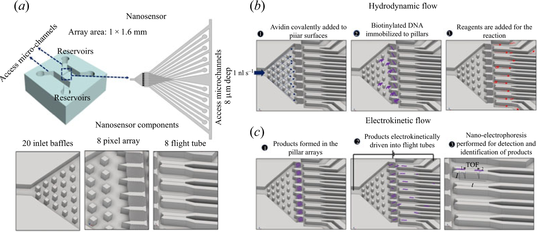
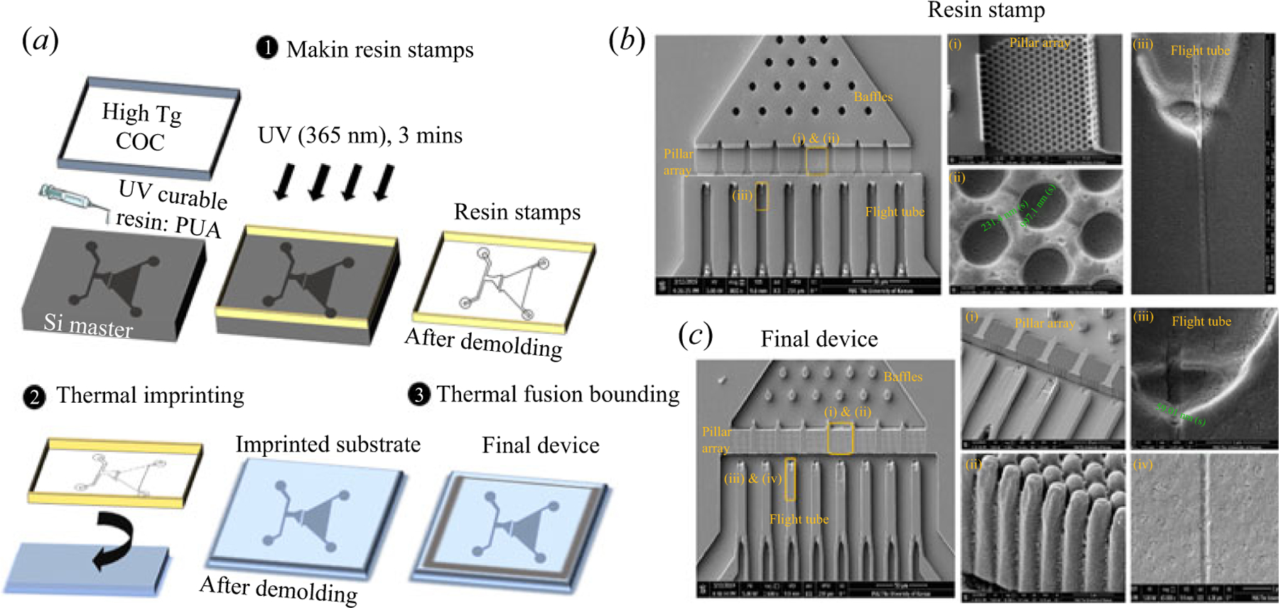
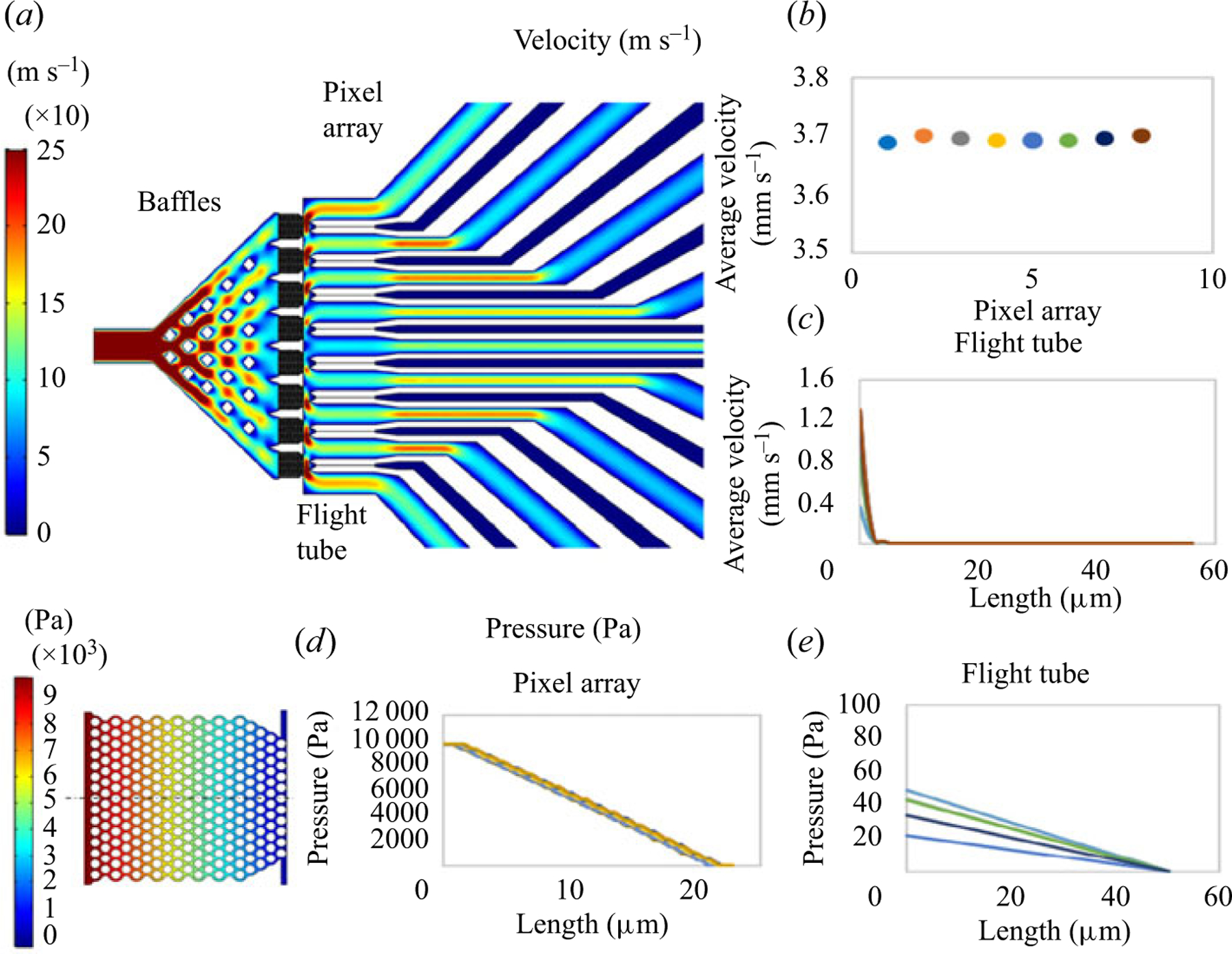
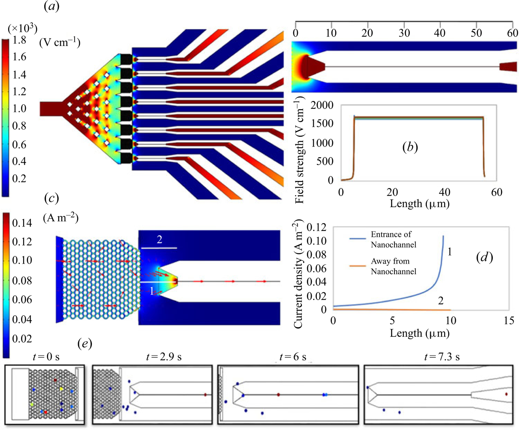
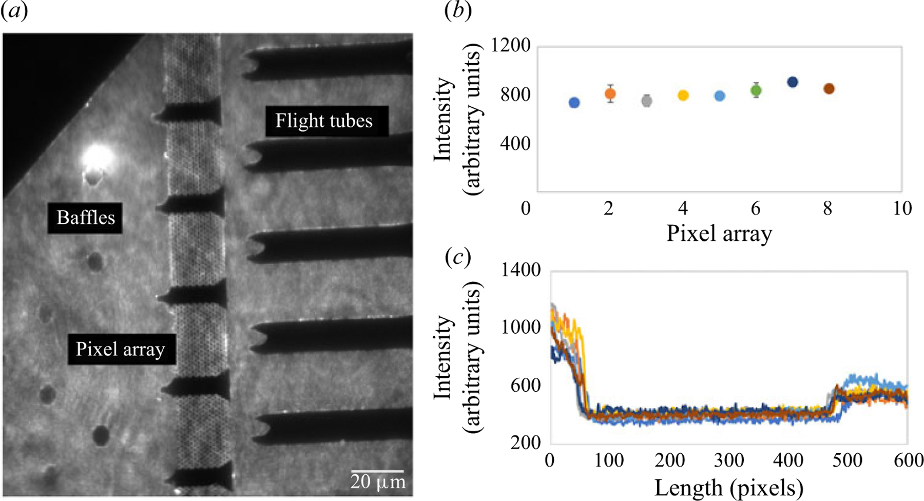
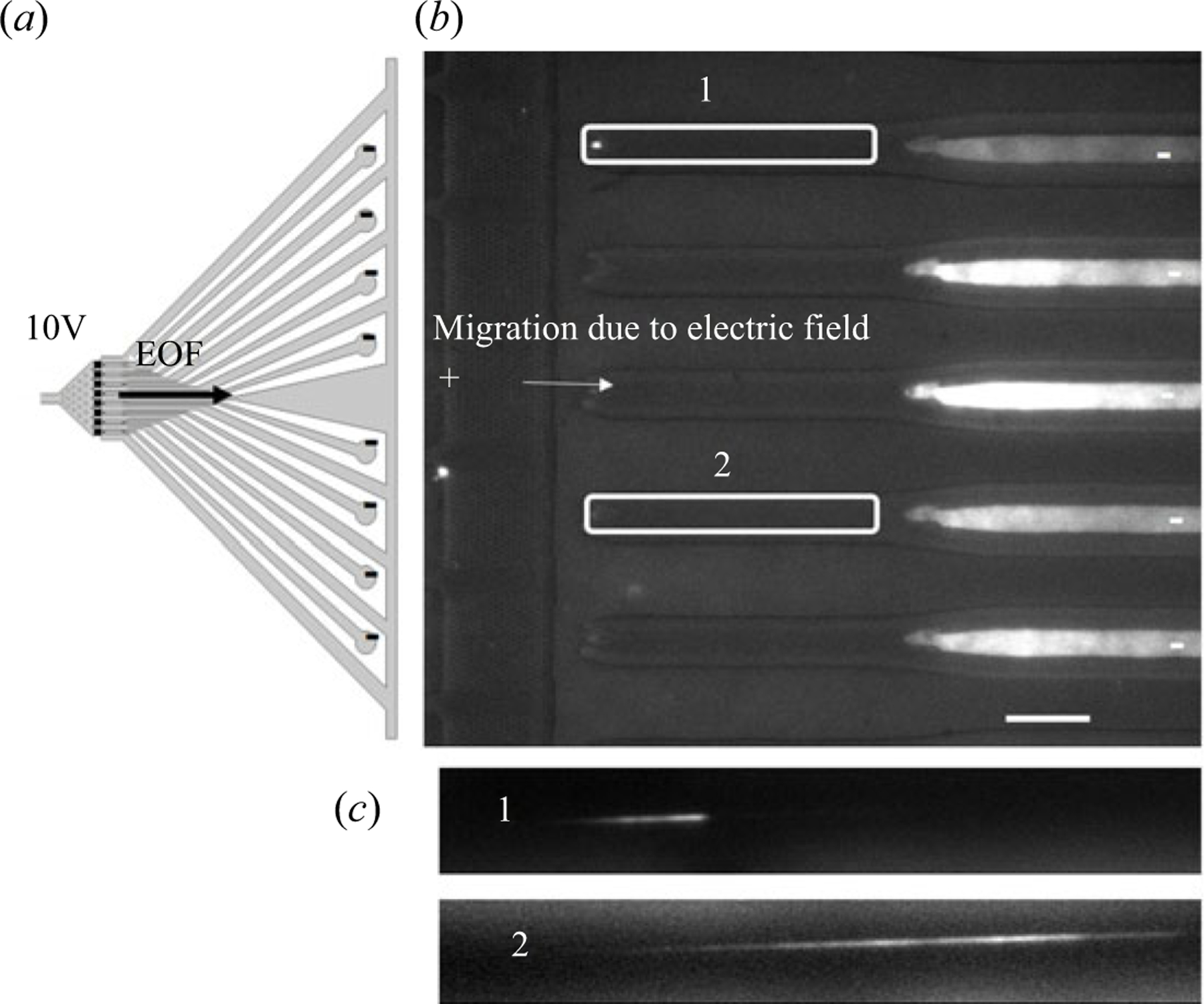
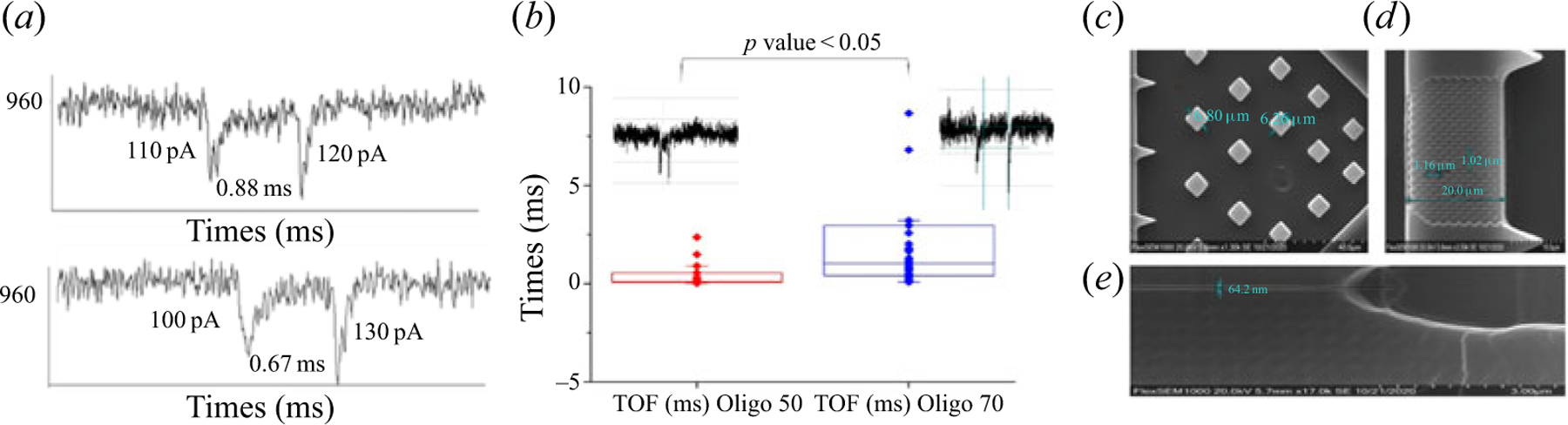
Most medical diagnostic tests are expensive, involve slow turnaround times from centralized laboratories and require highly specialized equipment with seasoned technicians to carry out the assay. To facilitate realization of precision medicine at the point of care, we have developed a mixed-scale nanosensor chip featuring high surface area pillar arrays where solid-phase reactions can be performed to detect and identify nucleic acid targets found in diseased patients. Products formed can be identified and detected using a polymer nanofluidic channel. To guide delivery of this platform, we discuss the operation of various components of the device and simulations (COMSOL) used to guide the design by investigating parameters such as pillar array loading, and hydrodynamic and electrokinetic flows. The fabrication of the nanosensor is discussed, which was performed using a silicon (Si) master patterned with a combination of focused ion beam milling and photolithography with deep reactive ion etching. The mixed-scale patterns were transferred into a thermoplastic via thermal nanoimprint lithography, which facilitated fabrication of the nanosensor chip making it appropriate for in vitro diagnostics. The results from COMSOL were experimentally verified for hydrodynamic flow using Rhodamine B as a fluorescent tracer and electrokinetic flow using single fluorescently labelled oligonucleotides (single-stranded DNAs, ssDNAs).

Keywords: Electrokinetic flow; Hydrodynamic flow; Plastic nanofluidics; in vitro diagnostics.


Conflict of interest statement

Conflicts of Interest. The authors declare no conflict of interest.

Figures

Figure 1.
Figure 1.
(a) Schematic of the nanosensor. The nanosensor is placed between two micrometre-sized access channels and is comprised of three main features; 20 baffles of 7 μm ×7 μm each to distribute reagents; 8-pillar arrays containing 268 pillars/array to perform solid-phase biological reactions; and 8 nano-tubes of 50 nm × 50 nm × 50 μm (w × d × l). (b) Sample processing steps carried out by the nanosensor that are enabled by hydrodynamic flow, which included pumping reagents (avidin) required for the solid-phase reactions (1); target DNA molecules immobilized onto the pillars of the array (2); and solid-phase reactions performed by adding the necessary reagents (3). (c) Electrokinetic flow is performed on the nanosensor chip and in the first step, the reaction is performed (1) followed by the products electrokinetically driven into the flight tubes through application of a DC voltage by placing electrodes at the end of the microchannel and grounding the ends of each nano-tube (2). Finally, once the products enter the nano-tube, they are detected using electrical measurements and the time-of-flight deduced for single DNA molecules to allow for their identification (3).
Figure 2.
Figure 2.
(a) Schematic of the fabrication and assembly steps of the nanosensor, which consists of 3 steps: (1) creation of resin stamps from the Si master by UV-NIL; (2) imprinting (thermal NIL) of the PMMA substrate using the resin stamp at 135°C, 300 psi, and for 5 min; and (3) thermal fusion bonding of a COC 8007 cover plate to the fluidic substrate at 70°C and 120 psi for 15 min. (b) SEMs showing the UV resin stamp where the structures were formed from the Si master. The pillar arrays (a) and their individual pillars (b), and the nano-tubes (c) were transferred into the PMMA substrate. (c) SEMs of the final PMMA device after thermal imprinting that has structures similar to the original Si master. The final device with the pillar arrays (a), the side profile of the pillars (b), the funnel entrance to the nano-tubes (c) and the nano-tubes (d).
Figure 3.
Figure 3.
(a) COMSOL simulation of hydrodynamic flow of 1× TBE through the nanosensor device at a flow rate of 1 nl s−1. The entrance of the nanosensor (25 μm) is used as the common inlet of the sampling/reagents. The flow entering the nanosensor is distributed uniformly across the pillar arrays by the baffles such that all 8 pillar arrays receive a constant delivery of the input fluid. (b) Graph showing the simulated average velocity across the 8-pillar arrays, which is ~3.7 mm s−1. The velocity across the 8 pillar arrays possessed a standard deviation of 6 μm s−1 between the arrays. (c) Hydrodynamic flow across the 8 nano-tubes, where the flow was found to be negligible. This is empirically represented in the line graph that is drawn across the flight tubes, where the velocity at the entrance of the nano-tubes dropped to ~0 mm s−1. (d) Pressure drop across the pillar arrays, where the average pressure drop among the 8 pillar arrays were found to be similar. (e) The pressure drop across the 8 nanochannel nano-tubes with respect to the pressure drop seen in the microchannels that are between the nano-tubes.
Figure 4.
Figure 4.
COMSOL simulation of electrokinetic flow through the nanosensor device. (a) Representation of the electric field strength across the nanosensor. A potential of 10 V was applied at the inlet of the nanosensor and each of the nano-tubes were placed at earth ground in their respective terminal reservoirs. The areas of the nanosensor having the smallest dimensions were found to have the highest electric field strength due to their higher fluidic resistance. (b) Contour and line plots of the electric field strength across the 8 nano-tubes. The electric field strength increased from the entrance and decreased at the output end and remained fairly constant through the majority of the nano-tube length. There was a similar electric field strength across the 8 nano-tubes, which was 1650 V cm−1. (c) Current density plot showing one pillar array and the nano-tube with arrows representing the direction of fluid movement and the length of arrows representing the field strength. (d) Line graph showing the current density up to 0.1 A m−2 at the entrance of the nano-tube and a drop in the current density to ~0.0015 A m−2 in the regions away from the nano-tube. (e) Particle tracing representative of ssDNA movement of 10 particles simulated in the pillar array (t = 0). The particles were observed to move preferentially into the nano-tube with more particles entering into the funnel (t = 2.9 s), and all of them translocating into the nano-tubes (t = 6 s). Those particles that are not in the funnel, but still in the radius of high current density were also drawn into the nano-tube (t = 7.3 s). The transfer efficiency (pillar array to nano-tube) was 80 % as deduced from the simulation results.
Figure 5.
Figure 5.
Experimental results of the hydrodynamic flow across the nanosensor. (a) Distribution of Rhodamine-B with hydrodynamic flow at a flow rate of 1 nl s−1. The dye was distributed across the pillar arrays by the baffles and preferentially into the microchannel areas surrounding the nano-tubes. No visible fluorescence was seen in the nano-tubes. (b) Fluorescence intensities across the 8 pillar arrays showing similar levels of intensities ranging from 800–950 (arbitrary units). The intensities were represented as grey-scale values. (c) The fluorescence intensity of the dye tracer was also evaluated in the nano-tubes, and a significant intensity drop was seen in the 8 nano-tubes. Areas having dye had a grey value >800, while the intensity in the nanochannels were ~300. The measurements were taken from 5 different experiments and used to calculate the mean and standard deviation. No statistically significant difference was observed between the intensity in the pillar arrays (p < 0.01 at 95 % CI). A scale bar of 20 μm is represented in the images. The fluorescence was captured using a sCMOS camera at an exposure time of 10 ms with the fluorescence collected using a 100× oil immersion objective. For the fluorescence measurements, the fluorescence intensity from the image in the presence of dye was measured in arbitrary units (14-bit camera setting; 16 384-grey-scale image) from the imaging camera and the background signal, also measured in arbitrary units with the same grey scale, was subtracted from the dye measurements.
Figure 6.
Figure 6.
(a) Schematic of the application of the DC bias voltage across the nanosensor. The 10 V potential was applied at the microchannel entrance to the nanosensor, while the ends of the nanochannel nano-tubes were placed at earth ground. (b) Fluorescent images showing the accumulation of fluorescently labelled ssDNA (25 nucleotides in length) from the pillar array to the end of each of the nano-tubes, but not in the microchannels flanking each nano-tube. (c) The nano-tube images were collected using a sCMOS camera with ROIs 1 and 2 showing a single ssDNA molecule in the nano-tube. A scale bar of 20 μm is represented in the images. The applied voltage was −10 V at the inlet with 100 mW laser intensity (532 nm excitation) and a sCMOS gain of 3 with 1 × 1 binning. The sCMOS camera was operated in a 14-bit mode.
Figure 7.
Figure 7.
(a) Representative traces of oligonucleotide 70 showing two peaks as they pass through the two nanopores placed in series, having a TOF of 0.88 and 0.67 ms. The numbers listed (pA) represent the current transient amplitude. (b) Difference in TOF between an oligonucleotide with 50 nt and one with 70 nt (p < 0.05). (c–e) SEMs for nano-injection moulding of the nanosensor. The three regions shown are the baffle region (c), The pixel array with the pillars are shown in region (d), which was comprised of 268 1-μm diameter pillars that were 5 μm tall, the nano-flight tube which is 50 nm width and depth and 50 μm long are shown in (e).

Similar articles

References

    1. Amarasekara CA, Athapattu US, Rathnayaka C, Choi J, Park S, & Soper SA (2020). Open-tubular nanoelectrochromatography (OT-NEC): Gel-free separation of single stranded DNAs (ssDNAs) in thermoplastic nanochannels. Electrophoresis, 41(18–19), 1627–1640. - PMC - PubMed
    1. Chou SY, Krauss PR, & Renstrom PJ (1995). Imprint of sub-25 nm vias and trenches in polymers. Applied Physics Letters, 67(21), 3114–3116.
    1. Chou SY, Krauss PR, & Renstrom PJ (1996). Nanoimprint lithography. Journal of Vacuum Science and Technology B, 14(6), 4129–4133.
    1. Dhawan AP, Heetderks WJ, Pavel M, Acharya S, Akay M, Mairal A, . . . Bhargava B (2015). Current and future challenges in point-of-care technologies: A paradigm-shift in affordable global healthcare with personalized and preventive medicine. IEEE Journal of Translational Engineering in Health and Medicine, 3, 2800110. - PMC - PubMed
    1. Kooy N, Mohamed K, Pin LT, & Guan OS (2014). A review of roll-to-roll nanoimprint lithography. Nanoscale Research Letters, 9, 320. - PMC - PubMed

LinkOut - more resources