

Chemical Vapor Deposition of Uniform and Large-Domain Molybdenum Disulfide Crystals on Glass/Al2O3 Substrates
- PMID: 35957148
- PMCID: PMC9370393
- DOI: 10.3390/nano12152719
Chemical Vapor Deposition of Uniform and Large-Domain Molybdenum Disulfide Crystals on Glass/Al2O3 Substrates
Abstract
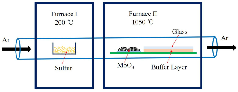
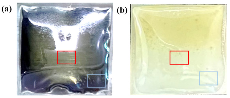
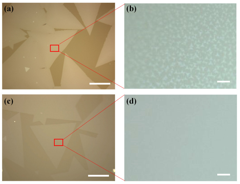
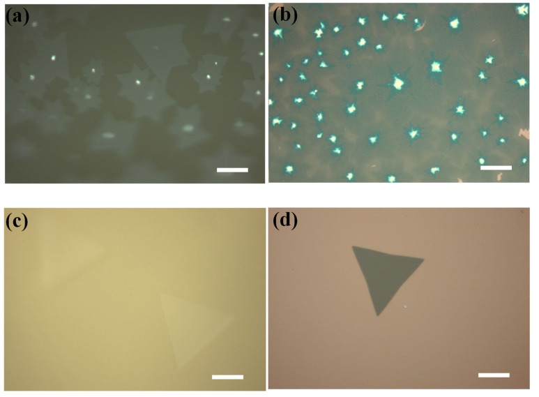
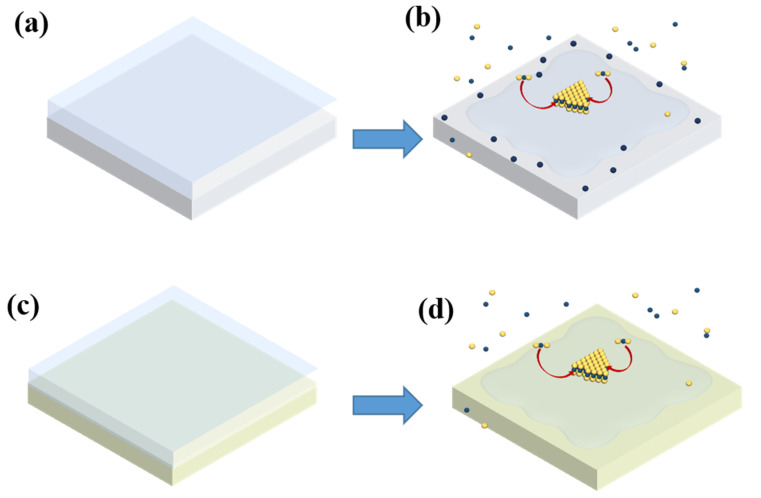
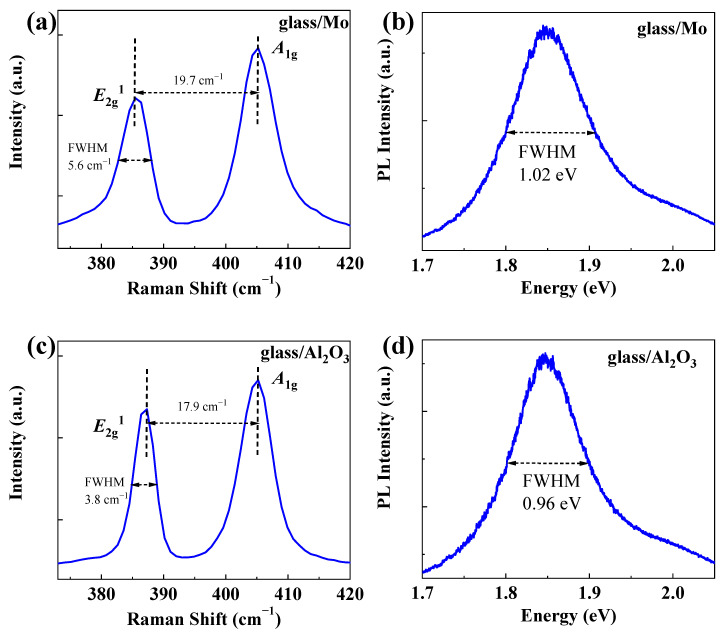
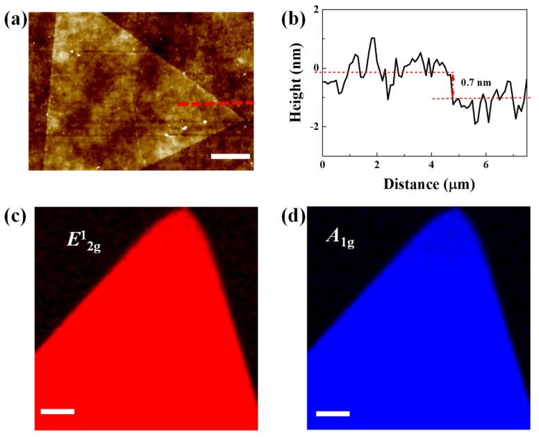
Two-dimensional molybdenum disulfide (MoS2) has attracted significant attention for next-generation electronics, flexible devices, and optical applications. Chemical vapor deposition is the most promising route for the production of large-scale, high-quality MoS2 films. Recently, the chemical vapor deposition of MoS2 films on soda-lime glass has attracted great attention due to its low cost, fast growth, and large domain size. Typically, a piece of Mo foil or graphite needs to be used as a buffer layer between the glass substrates and the CVD system to prevent the glass substrates from being fragmented. In this study, a novel method was developed for synthesizing MoS2 on glass substrates. Inert Al2O3 was used as the buffer layer and high-quality, uniform, triangular monolayer MoS2 crystals with domain sizes larger than 400 μm were obtained. To demonstrate the advantages of glass/Al2O3 substrates, a direct comparison of CVD MoS2 on glass/Mo and glass/Al2O3 substrates was performed. When Mo foil was used as the buffer layer, serried small bilayer islands and bright core centers could be observed on the MoS2 domains at the center and edges of glass substrates. As a control, uniform MoS2 crystals were obtained when Al2O3 was used as the buffer layer, both at the center and the edge of glass substrates. Raman and PL spectra were further characterized to show the merit of glass/Al2O3 substrates. In addition, the thickness of MoS2 domains was confirmed by an atomic force microscope and the uniformity of MoS2 domains was verified by Raman mapping. This work provides a novel method for CVD MoS2 growth on soda-lime glass and is helpful in realizing commercial applications of MoS2.
Keywords: MoS2; chemical vapor deposition; glass; substrate.
Conflict of interest statement
The authors declare no conflict of interest.
Figures
Similar articles
-
NaCl-Assisted Chemical Vapor Deposition of Large-Domain Bilayer MoS2 on Soda-Lime Glass.Nanomaterials (Basel). 2022 Aug 24;12(17):2913. doi: 10.3390/nano12172913. Nanomaterials (Basel). 2022. PMID: 36079950 Free PMC article.
-
Application-Oriented Growth of a Molybdenum Disulfide (MoS2) Single Layer by Means of Parametrically Optimized Chemical Vapor Deposition.Materials (Basel). 2020 Jun 20;13(12):2786. doi: 10.3390/ma13122786. Materials (Basel). 2020. PMID: 32575719 Free PMC article.
-
Towards Low-Temperature CVD Synthesis and Characterization of Mono- or Few-Layer Molybdenum Disulfide.Micromachines (Basel). 2023 Sep 11;14(9):1758. doi: 10.3390/mi14091758. Micromachines (Basel). 2023. PMID: 37763921 Free PMC article.
-
A Novel Carbon-Assisted Chemical Vapor Deposition Growth of Large-Area Uniform Monolayer MoS2 and WS2.Nanomaterials (Basel). 2021 Sep 17;11(9):2423. doi: 10.3390/nano11092423. Nanomaterials (Basel). 2021. PMID: 34578743 Free PMC article.
-
Emerging MoS2 Wafer-Scale Technique for Integrated Circuits.Nanomicro Lett. 2023 Jan 18;15(1):38. doi: 10.1007/s40820-022-01010-4. Nanomicro Lett. 2023. PMID: 36652150 Free PMC article. Review.
Cited by
-
NaCl-Assisted Chemical Vapor Deposition of Large-Domain Bilayer MoS2 on Soda-Lime Glass.Nanomaterials (Basel). 2022 Aug 24;12(17):2913. doi: 10.3390/nano12172913. Nanomaterials (Basel). 2022. PMID: 36079950 Free PMC article.
References
Grants and funding
- 62104033, 62071088 and 11775047/National Natural Science Foundation of China
- 2019A1515110752/Guangdong Basic and Applied Basic Research Foundation
- 2019KQNCX187/Youth Innovative Talent Project of Guangdong Education Department
- 2019/Outstanding Chinese and Foreign Youth Exchange Program of China Association for Science and Technology (CAST)
- 2018KCXTD033, 2020KCXTD030 and 2021KCXTD040/Project for Innovation Team of Guangdong University
LinkOut - more resources
Full Text Sources
Research Materials
